24V Dc to 220 V Ac Inverter @ 65 Khz Using IC TL494 30Watt
by rupjit81 in Circuits > Electronics
101 Views, 1 Favorites, 0 Comments
24V Dc to 220 V Ac Inverter @ 65 Khz Using IC TL494 30Watt

In this design Im designing and testing an inverter 24V dc to 220 V ac inverter @ 65 khz. The control circuit is based on IC TL494. The operating frequency at transformer secondary is 65 khz.
Im using mosfet IRF840 as the power switch.
I have powered a lamp at output.
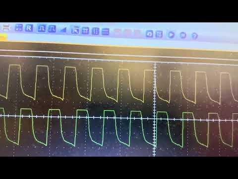
The PWM function has been tested by varying the input vol
Supplies
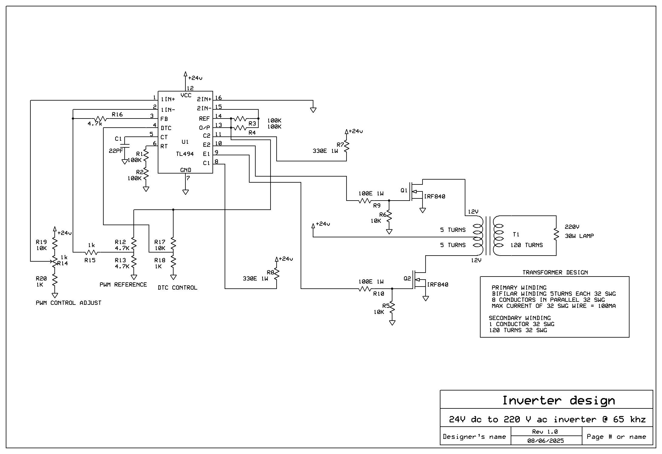
BILL OF MATERIALS
C1 22PF
Q1 IRF840
Q2 IRF840
R1 100K
R2 100K
R3 100K
R4 100K
R5 10K
R6 10K
R7 330E 1W
R8 330E 1W
R9 100E 1W
R10 100E 1W
R11 30W LAMP
R12 4.7K
R13 4.7K
R14 1k
R15 1k
R16 4.7k
R17 10K
R18 1K
R19 10K
R20 1K
T1
U1 TL494
Construction


Please follow the circuit diagram as reference.
The design uses IC TL494 as the heart of the circuit.
Pin 11 and pin 8 of collector is pulled up to 330 ohm 1 W resistor. R7 and R8 in circuit diagram.
Pin 9 and 10 are emitter pins and they are connected to 100 ohm 1 W resistor. R9 and R10 in diagram.
R5 and R6 are 10k resistors used to discharge the gate capacitance of MOSFET Q1 and Q2 Both IRF840 in diagram.
MOSFETs Q1 and Q2 are IRF840 used as power switch. Suitable heatsink must be provided to radiate the heat.
Both MOSFET drains are connected to the transformer T1 primary windings. The center tap is connected to 24V DC supply.
The transformer secondary is connected to the load.
IC TL494 pin 5 is connected to capacitor C1 of 22pf and pin 6 is connected to two 100k resistances in series named R1 and R2 in circuit.
Pin 13 and 14 is shorted that makes sure pin 9 and 10 are out of phase.
Pin 4 is the dead time control pin between two pulses. It is controlled by R17 and R18 10k and 1k voltage divider network.
Pin 3 is the feedback pin. Pin 1 and 2 are non inverting and inverting pins of OPAMP inside TL494.
R15 and R16 makes a gain of nearly 5. [4.7k / 1k i.e. R16/R15].
R12 and R13 gives a reference voltage of 2.5 V and feeds to TL494 opamp pin 2 via R15 and R16.
R19, R14 and R20 gives the PWM reference on pin 1 of TL494.
Pin 16 is grounded in this design. Pin 15 is connected to R3 and R4 100k in parallel.
This design has no over current trip. This will be included in later designs.
Transformer Design

Note that the transformer is designed to operate in primary 12 - 0 - 12 V AC or 24 V AC.
The primary is a bifilar winding with center tap connected to 24 V
The other two ends of transformer are connected to mosfet Q1 and Q2 drains.
Primary winding is 12 - 0 - 12 , 5 turns bifilar winding.
32 SWG copper wire 8 conductors together.
Secondary winding is 120 turns 32 SWG copper wire
Conclusion
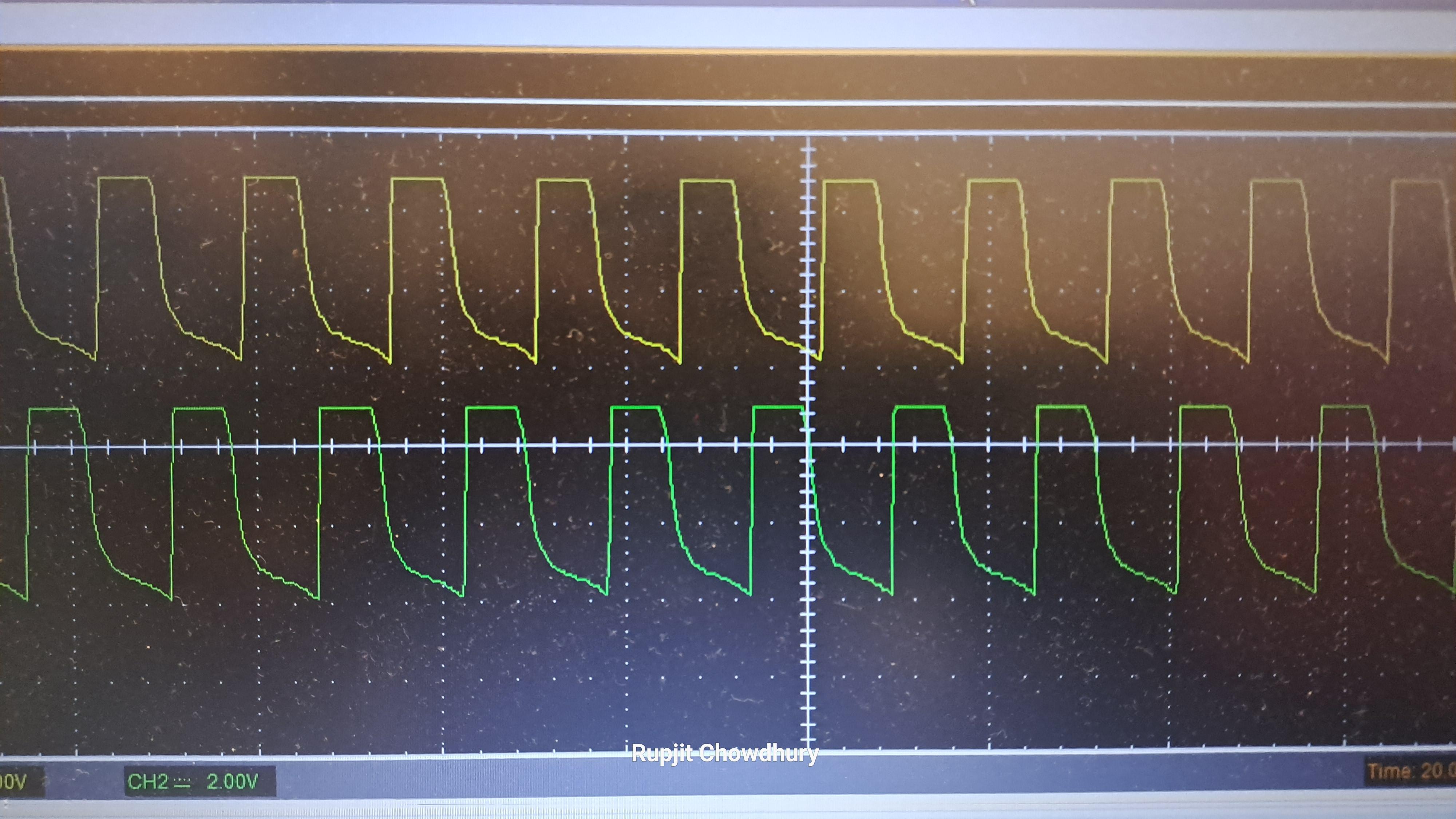


The circuit outputs 220V AC @ 65 KHZ. There is a risk of electric shock.