Arduino ISP to ATTiny85


When I discovered the ATTiny range of Atmel chips, I was excited to learn that many of the projects that I had planned could be achieved with the small and inexpensive chip. There are many instructables and tutorials on the interweb that describe projects using the ATTiny chip.
The two chips that I use are the ATTiny85 (8 pin) and the ATTiny84 (14 pin). Usually, I use the ATTiny85 more than I use the ATTiny84, but that's mostly because when I am using these reduced footprint microprocessors, I'm trying for the smallest footprint possible.
To program your ATTiny85, the most straightforward way is to connect it to your Arduino Uno (or clone) and use the Uno as an In Circuit Serial Programmer (ICSP or ISP).
In this instructable, I'll show you how to make your own Uno Shield (plug-in component) that allows you to drop your ATTiny85 into the shield and program it.
I've used my ATTiny85 shield on several projects so far and it has run without a hitch.
Preparation and Materials List


The materials used in this project are pretty few.
You will need:
- 1 x 40mm x 53.5mm single sided copper clad circuit board (FR4)
- 12 x pin headers (cut into 2, 4 and 6 pins)
- 1 x 8 pin DIL socket
- 3 x 220 ohm resistors
- 3 x 3mm LED (green, red and blue)
I've used the toner transfer and acid etch technique for making the board, but you can use whatever method best suits your skills and budget.
You will also need a circuit design program to draw your circuit. I use the free Fritzing designer tool, it's great, has the components that I need, is easy to use and it's free (did I mention that it is free?).
Toner Transfer Method (abridged)
The toner transfer method is simply about melting the toner from a laser printout onto the copper of your circuit board. The toner acts as an acid resist, meaning that when the board is immersed in acid, the copper that does not have the resist on it, will be etched away by the acid.
- Design your circuit
- Print your design on plain paper with a laser printer
- Transfer the image onto the copper with a hot iron (for 3-4 minutes)
- Clean the copper clad board. While the copper is still hot, drop it into a hot bath of water. Peel the paper off and rub the paper residue from the board with your fingers.
Acid Etch Method (abridged)
Actually, there are plenty of them ... here's the recipe that I use.
- 2 parts hydrogen peroxide
- 1 part hydrochloric acid
Keep a bath of salty water handy, your salty water should be a 100% saline solution, that means that you cannot dissolve any more salt into the water. The saline solution is used to neutralize any acid that gets where it shouldn't. You should, of course, be using rubber gloves and eye protection AT LEAST. Acid is dangerous stuff.
Also, when you do your acid etching, do it somewhere that has good ventilation, the etching process releases toxic gasses and they can be harmful.
Also ... no children, no pets, no distractions ... accidents can happen.
I make up just enough etchant for my job. It doesn't have a good shelf life and I don't like being wasteful. Also, limiting the amount of acid I'm playing with limits the possible results of an accident. As a rule of thumb, I tend to mix up about 1/3 of a cup of etchant for a job this size. I also have a couple of jobs ready so that I can use the acid etch all at once. Planning ;) I use a (thoroughly clean) plastic butter container or ice-cream container for my acid bath.
Immerse your PCB into the acid etch and gently tilt the bath back and forth left to right switching to forward and backward (being careful that the acid doesn't slosh out of the container). Agitating the acid bath makes it work faster by removing the etched particles into the solution. If you don't agitate, it will still work, it'll just take longer.
The copper will darken and then gradually fade from the backing board. Using the agitation method, this is visible, using the non-agitation method ... 3 to 4 times longer.
When the copper has dissolved from the board, take it out and immerse it in the saline solution. Just a quick dip and swish. Then, run the PCB under running water. The acid will continue to etch the board after you have removed it from the bath, it's important to thoroughly clean the acid from the board.
Bread Board It


The first thing that you want to do is to test your wiring. This is pretty simple, really.
Plug the ATTiny85 into a breadboard, a half-size will do just fine.
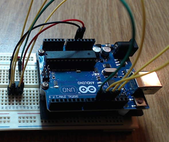
If you open your Arduino IDE and then click File -> Examples -> ArduinoISP, the ArduinoISP sketch is loaded into the IDE. This is very useful as it tells you how to connect the Arduino to the ATTiny85 (also for the Mega 1280 and 2560, if you are so inclined).
Arduino Uno to ATTiny85 Connections
- Arduino 5V connects to ATTiny85 Pin 8 (Vcc)
- Arduino GND connects to ATTiny85 Pin 4 (GND)
- Arduino Pin 13 connects to ATTiny85 Pin 7 (SCK)
- Arduino Pin 12 connects to ATTiny85 Pin 6 (MISO)
- Arduino Pin 11 connects to ATTiny85 Pin 5 (MOSI)
- Arduino Pin 10 connects to ATTiny85 Pin 1 (Slave Reset)
That's all of the connections from the UNO to the ATTiny85.
Prepare the UNO
The Arduino UNO needs to be programmed to work as a ICSP. This is done very easily using the ArduinoISP example sketch.
When you have connected your ATTiny85 to the UNO according to the previous step, the next stage is programming the UNO.
- Open the sketch File > Examples > ArduinoISP
- Make sure the UNO is the target board Tools > Board > Arduino UNO
- Make sure the UNO is using the right programmer Tools > Programmer > AVR ISP
- Verify the sketch (not 100% necessary, but always a good practice) Sketch > Verify/Compile
- Upload the ArduinoISP sketch to the board File > Upload
Now, at this stage, you will probably get the perennial false negative warning about the AVRDUDE - PAGEL BS2. You can ignore that warning if you like ... or you can fix it ... forever. I found the solution to this problem a while back and I wrote an article on my blog about how to resolve the warning. Go check out the solution on my blog here. It's a bit tricky because you have to edit the avrdude.conf file and make changes to it ... anyway, back to the instructable.
The Arduino UNO is now ready to be used to program the ATTiny85.
Make It Blink
One of the things that I found when I was reading through the ArduinoISP example sketch is that the clever designer (Randall Bohn) included LED indicators in his sketch for:
- Heartbeat - pulsing LED showing that the ICSP is ready
- Error - flashes when the ICSP encounters and error while uploading
- Programming - flashes when the ICSP is receiving programming instructions
Wiring up the indicator LED is a pretty straight forward process. If you open the attached Fritzing design, you will see that I've got the LED attached thus:
- Heartbeat (3mm Green LED) connects to Pin 9 of the UNO
- Error (3mm Red LED) connects to Pin 8 of the UNO
- Programming (3mm Blue LED) connects to pin 7 of the UNO
The connection from UNO to LED is via a 220 ohm resistor and to the GND of the UNO on the negative leg of the LED.
This is not essential, however, if you are making a permanent ICSP shield, it's nice to have some visual indication of progress, so I'd recommend that you do. Besides, LED and resistors are cheap and there is plenty of real-estate on the board.
Downloads
Make the PCB


Using the Fritzing sketch from the previous step, print out both silk side and the copper side on your laser printer.
Using the toner transfer method described in step 1, transfer the copper trace to the copper side of your PCB and etch it.
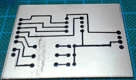
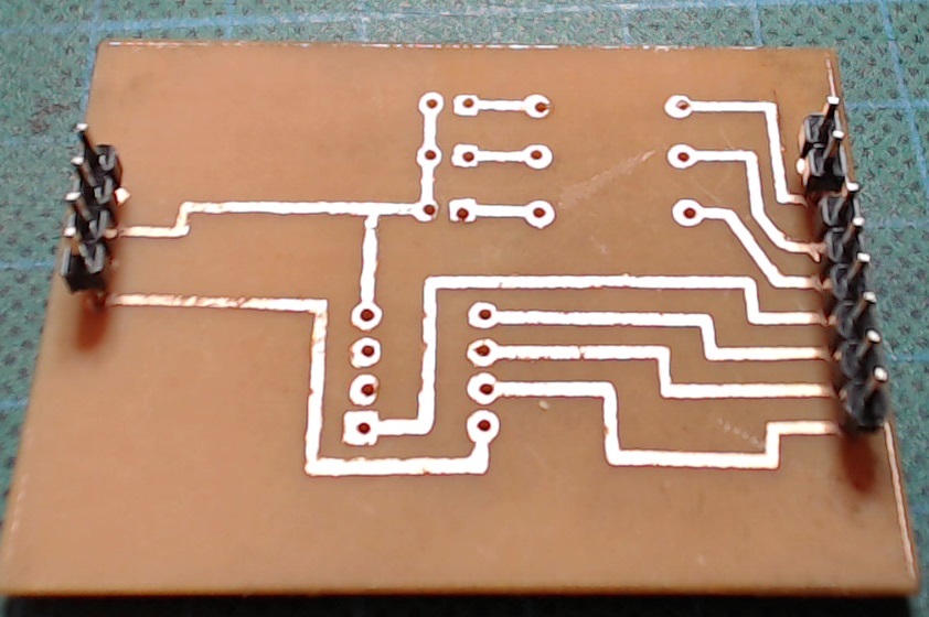
The three images above shows
- Copper side with toner transferred
- Copper side after etching with toner still attached
- Copper side after etching and with toner removed with acetone.
There are a couple of tricks that will make your life easier and your production better.
After transferring the toner to the copper side of the board, go over the toner with a permanent marker. You want a permanent marker that deposits an ink that is water resistant (I have had a lot of luck with the Staedler LUMO Color Waterproof marker) I have Fine and Medium markers for this. The main reason that I do this is that the toner method is not perfect.
Use acetone to remove the toner from the PCB, this should leave your copper traces all bright and shiny.
Use a multimeter on continuity testing to test each of the traces from end to end. If you find holes in your traces, use a hot soldering iron and solder to bridge any gaps.
Drill the through holes with a 0.2 drill bit in a pin vice. Smaller is better.
Tin the pads with solder.
Retest the traces with your multimeter.
An ounce of prevention is worth a pound of cure.
After drilling my through holes, I then glue the silk side paper onto the silk side. I've looked at lots of different methods of home made silk printing on PCB and they are all too much cost and hassle for me. I simply spread white PVA (wood glue) onto the surface and then stick the paper on. I then lacquer the paper with more PVA until it is well covered. I then use a fine awl and poke the holes through the paper from the copper side so that I end up with a nice laser printed silk print on the top of my PCB. I think it looks good, personally, you may disagree ... it's entirely up to you, whether or not you do this.
After that, it's simply a matter of soldering in your components.
When I came to soldering in the pin headers, I wanted to make them look good. How I did this is that I first pushed the plastic block down to the other end of the pins and inserted the pins into the copper side of the PCB (so that they went through the PCB but didn't protrude on the silk side). Next, I carefully soldered in the pins leaving as little fillet of solder as possible (a small rat tail file helped when I had too much, followed by some copper braid to clean up). Then I pushed the plastic block back down so that it was tight to the PCB. You should also know that there are more pins than there are traces. I've got 2 extra pins on the left-hand side and one extra on the right-hand side. I included these pins for mechanical strength and stability. Without those extra pins, the left-hand side tends to bend when removing the shield from the UNO.
When the soldering is done, it's back out with the multimeter and test the continuity of each trace from pin to DIL and pin to LED ... in fact ... test everything.
Have a Moment to Enjoy Your Results.


Now that the board is all soldered and lacquered, it looks pretty smart. I also went to the trouble of painting some black paint around the edge of the board so that it looks pretty.
If you plug your shield into your UNO and connect it to power (either through the DC connection or using the USB connection) and if the ArduinoISP sketch has been uploaded to the UNO, your heartbeat LED should pulse showing you that it is all tickety-boo.
You should be pretty happy with yourself, you've made a UNO shield with a few inexpensive components.
Program Your ATTiny85


In your Arduino IDE, open up the blink sketch (File > Examples > 01. Basics > Blink)
Change the pin in the sketch to pin 0.
The example sketch uses pin 13 and, since the ATTiny85 doesn't have one, we need to use a compatible pin. Pin 0 will do nicely.
You now need to tell the IDE that the ATTiny85 is the target board by selecting Tools > Boards > ATTiny85 (internal 1MHz clock)
Next, you need to tell the IDE that you are using ArduinoISP as the programmer by selecting Tools > Programmer > Arduino as ISP
Make sure that you have an ATTiny85 chip (correctly oriented) in the DIL on your board.
Verify the sketch (Sketch > Verify/Upload)
Upload the sketch (File > Upload Using Programmer)
Your blue LED should flicker as the program is uploaded to the ATTiny85.
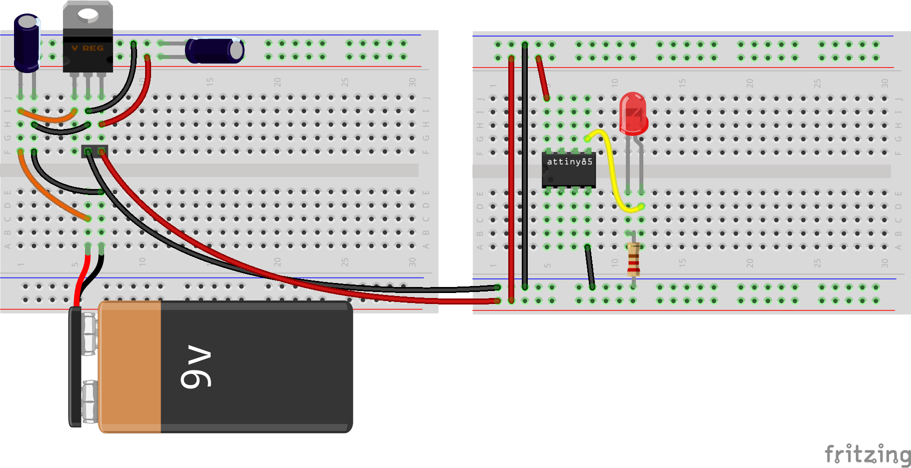
Connect your programmed ATTiny85 as per the above breadboard image. If you don't have the 5V regulator, simply connect the 5V and GND on your UNO to the breadboard to provide you with power. When the power is up and your components are breadboarded, your LED should blink like the little blinker that it is.