Big Seven Segment Display

Ever since I had solar panels installed on my roof I wanted a display showing the power they generate. The setup I have can produce up to about 3 kW so four digits is needed.
I want it to be visible from a few meters distant so a small LCD, OLED or LED display isn't good enough. I also has to be bright enough to be readable in bright sunlight. Of course I can go out and buy such a display but if I had done that, you wouldn't be reading this...
Most devices I make are for me only and so I never bothered to design a PCB for it. But in this case the idea of putting a large number of LEDs on perfboard and having to connect them all with wires is not something I was looking forward to do, so it has to become a PCB. So I did. But this brought up some design questions.
-
Design files and arduino code for testing can be downloaded from Gitlab.
-
Supplies
Kicad Schematic Capture & PCB Design Software
Per Digit:
28 x Cree J5630 led
2 x Capacitor 100nF 0805SMD
1 x Resistor 1k ohm 0805SMD
4 x Resistor 100k ohm 0805SMD
1 x pinheader 6 pins right angle
1 x pinsocket 6 sockets right angle
1 x STP16CP05 (led driver)
1 x APE8865N (3.3V linear regulator)
1 x PCB (made by PCB manufacturer)
Matrix or Seven Segment
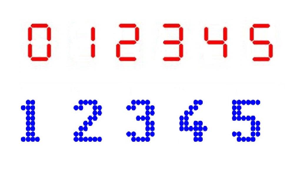
Do I go for a seven segment display or a matrix of leds, e.g. 7 x 5 or 8 x 6 leds.
I made a number of test designs and decided that for visibility versus complexity a seven segment display was best. In my final design a seven segment digit uses 28 leds and the number "1" has 8 leds.
To have the same number of leds for the number "1" with a matrix design a single digit would have to have 8 x 6 = 48 leds at least! Although the shape of numbers with a matrix design looks better, I chose the seven segment option.
Size Vs Cost


Here the prices the PCB manufacturers charge are important. Most have a special (low) price for PCBs up to 100mm x 100mm (double sided). For maximum flexibility I want every digit on a separate PCB, that way I can combine them in any number of digits.
After some measuring I decided to put two digits on one 100mm x 100mm PCB and ask the manufacturer to mill a, so called, V-score in the middle of the PCB. (See picture and more about this later)
So one digit has 100mm x 50mm PCB-space available. But a digit in those dimensions (in my opinion) is ugly so I reduced it to 80mm x 50mm. The rest of the PCB can then be used for connectors and mounting holes. An advantage of making separate digits is that I can use them for other things than only a display for my solar panels.
Type of LEDs
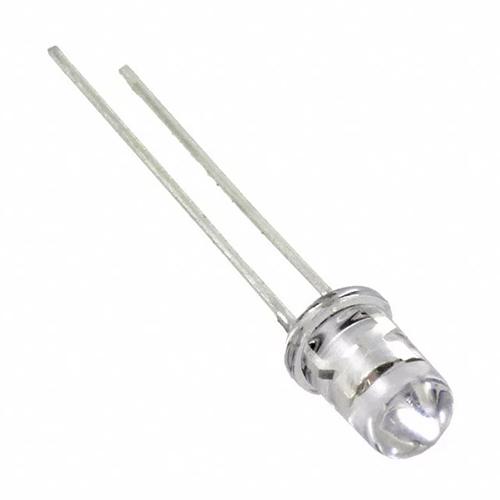
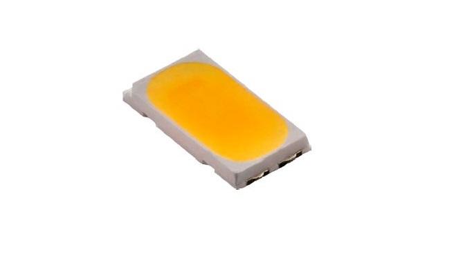
Then I had to decide what type of leds to use, through-hole? smd? colour? brightness? openings angle? size?
The display has to be visible from many places, so the openings angle of the leds has to be as wide as possible. That almost immediately ruled out most through-hole leds, and wasn't too happy about using those anyway as it makes the display much thicker, so smd leds. The colour was easy: white. With white you can have any colour you want be putting a perspex screen of the colour you like in front of it. Brighness was in part a matter of price, the more light, the higher the price. The other part is the maximum current (power) to use for the leds.
Cree solved this problem when I found the Cree 5630 leds. They are VERY bright at a modest current of 65mA (max pulsed current 240mA). And it also solved the question of the size, these leds are rectangular, perfect for a seven segment display. You may wonder why I didn't use WS2812 RGB LEDs or strips of those (sometimes called neopixels), the reason is both price and the fact that I don't care for changing the colour of the display "on the fly". I simply want a display, not some carnival attraction.
Led Driver
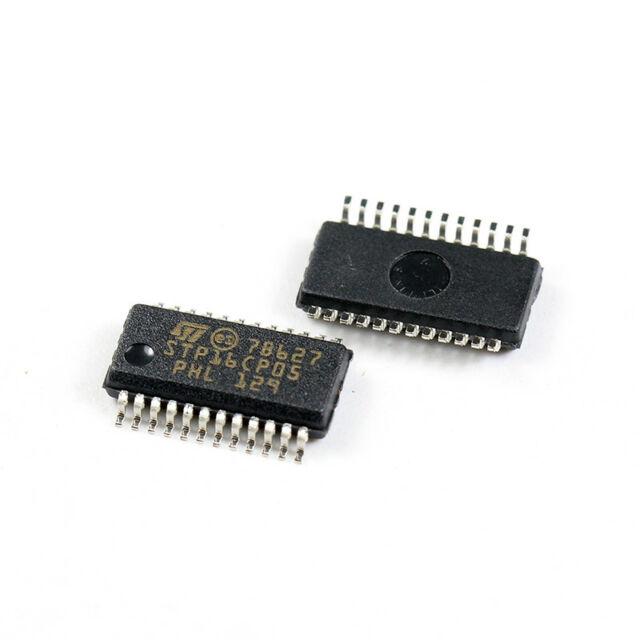

Next question: the driver. For the choice of driver you need to think about how you are going to arrange the leds and how you want to control the driver. Use all the LEDs in parallel, all in series or a combination of that. One segment in this display has 4 (white) leds, if put in series they would need 4 x 3V = 12V, but you need some extra voltage for the driver itself, so it would become someting like 14V. An advantage of this methode is that you need a driver with just 7 channels.
Using all leds in parallel asks for just 4 of 5V but also a driver with 28 channels. I went for the compomise of 2 leds in series split each segment is two parts. Now those two LEDs in series needs 7 to 8V but a driver with 14 channels. STMicroelectronics makes a nice 16 channel driver, the STP16CP05, with a current sink for each channel that works from 3 up to 20V, the current can be set with a single resistor from 5 to 100mA. And it can be controlled with a microcontroller using SPI and running on 3.3V. Controlling with SPI is easy, perfect!
Schematic
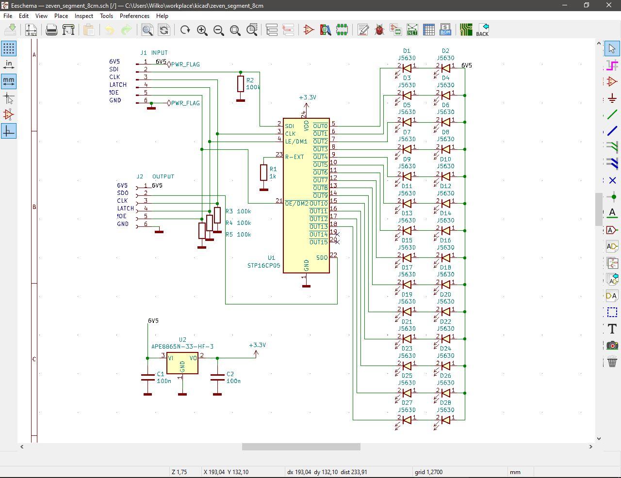
For designing the PCB I used Kicad as I am already used to it for drawing my schematics. I won't bother you with the installation as it is pretty straight forward. First of all create a new project and go into the schematic editor.
Connect the parts with the Wire-Symbol (single green line). Don't forget to add power to the active parts and also don't forget to place a No-Connect_Symbol (blue cross) to pins you do not connect to anything else.
If you place the cursor obve a compoment and press the letter "V" you can give it a value, such as 10k for a resistor. This can also be done with the letter "E" with gives many more options, usually "V" is enough. There is much more to tell about the schematic editor of Kicad (and all parts of the program) but I will not go into that, just keep experimenting with all options until you are happy with the result. I doubt that I use more than 10% of what is possible, but it gets the job done.
A realy short Cheat-Sheet that makes up most of what I need is this: V - give or change value E - edit C - copy M - move
Annotate and the Electric Rule Checker


Annotate all components (Paper-And_Pencil symbol) so that they no longer are called R? C? and so on.
Start the "Electrical Rule Checker" (ladybird) when you think you are done with the schematic and press "Run". This will check for errors in the schematic such as unconnected pins of an IC, shorts and other problems. One annoying problem can be that it wants to see that you really power active devices. This can be fixed by placing a "Power-Flag" on a wire that will (leter) be connected to a power source.
Assigning Footprints

And then start the "Assign PCB footprints to schematic symbols" (opamp-ic-symbol) program to tell Kicad the size and shape of the componemts you selected. This part took me quite some time. I was (am) not very familiar with how the sizes of capacitors, resistors, ICs, etc are notated.
As an example a simple 1k resistor : Resistor_SMD:R_0805_2012Metric_Pad1.15x1.40mm_Handsolder"
And even worse is it when the footprint component you selected isn't in the database of Kicad. I had to make my own footprint for the LEDs. Only later I discovered that almost all footprints can be downloaded from places such as the producer of the part (in this case Cree) or from Kicad and there are even some sites that have thousands of footprints of all sorts of components that you download for free. (SnapEDA, Mouser, Sparkfun)
Laying Out the PCB
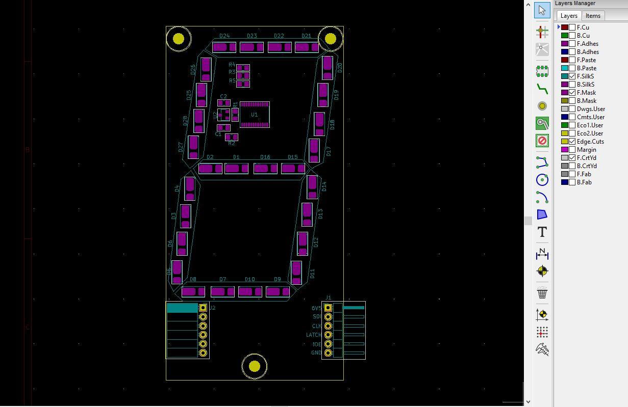
Next comes the REAL fun part, laying out the PCB...
Generate a netlist (icon with text NET), save it and start PCBNew (PCB symbol), open the Netlist you just made, ignore the fact that all components are shown in one big mess.
First you have to create the so called outline of the PCB. This you do with the Edge-Cuts layer. On the right side of the screen select this layer (a small triangle shows the active layer) then select "add graphic lines" (4 green dots connected with blue lines) Now you can draw the outline of the PCB you want to make. Again, experiment with the options available, I sometimes use the "measure distance" in this stage of the development. Also in this program I probably use less than 10% of all options.
The jobs really starts when you begin moving your components from the big mess they came in. I never put them directly to the place where I think they need to go. I first spread them out over the entire screen. This way you can see which component is connected to which other component. Then slowly I place some components to where I think they are placed best. Some parts will have fixed places of course, a connector usually goes to the edge of the board so you can place these first.
3D Viewer

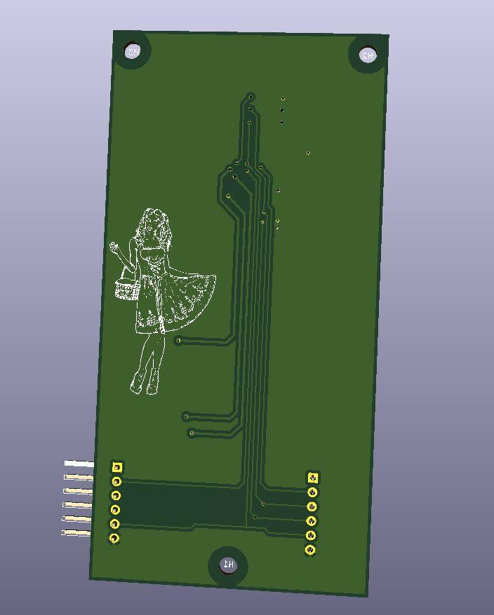
Very helpful is the 3D viewer, press ALT-3 to start it. With this you can see what the populated PCB looks like. You can start this program at any stage, even when most of the parts are not even on the board! Then "Grab" the board with your mouse and you can rotate, flip and move it all over the screen to look at it from all angles.
Connect the Components


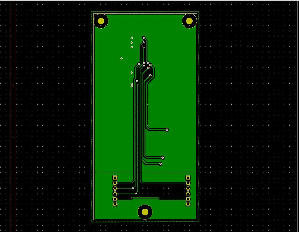
When the components are all in the place you want them to be, click the "route-track" icon and start connecting the pins of the components. As soon as you connect them (in the correct way) the temporary white lines start to disappear. You can place tracks on both sides of the (two layer) PCB and connect them with a "via". The first connection you make will be easy but it gradually will become more difficult as there will be more tracks in the way. For a simple design as this one two layers is more than enough. It could probably even be done on a single layer board, but surprisingly single sided boards are more expensive (in China).
The Design Rule Checker

When all tracks are done, run the "Design Rules Check" (ladybird) and
click "Run DRC" this with check if the tracks are not to close to each other, if they are not too thin, if the vias are okay. Also click "List Unconnected" to check if you forgot to connect some pins. The default values for these checks are good enough for having the board made by (most) PCB makers.
Gerber Files

The last thing to do is to create the (Gerber) files to send to the PCB maker, to do this, click "File - Plot" and plot all the default selected files. This usually is more than enough for the maker. After you upload the files to their website (and read their instructions) you can always take another good look at what the PCB will look like as they all have a tool to show the actual contents of your uploaded files.
A small warning. Some PCB makers will charge you (much) more if they see that you place one design two (or more) times on one PCB. In my case I wanted two displays on one 100mm x 100mm PCB with a V-score in the middle of the PCB. One maker increased the price FOUR-FOLD just to make this simple V-score. Another did it with out any extra costs.
There are many many more things to say about Kicad, you can change so many settings, tweak so many parameters, but that does not belong in this instructable, on youtube you can find videos with more explanations. I learned most from a seies of videos of "Contextual Electronics" and another whole series of video of "John's Basement"
Arrival!


Some time later your PCBs will arrive, check them before you start placing components for open connections, shorts or other defects I haven't had any problems with my designs, but it is better to be safe than sorry.
Soldering the Components and Testing


I didn't order a stencil for putting solder pasta on the boards as I (still) can solder all parts by hand. Even the STP16CP05 a component with its TSSOP24 footprint that has pins every 0.65mm can be soldered by hand. I do need glasses, a watchmaker-loupe and a lot of light though.... The way I work is to solder one pad on the PCB for all components, with tweezers move the component against this solder and heat both the pad and the pin of the component with my soldering iron. If the part is in the correct position, remove the iron and wait a few seconds. Then solder the other pin(s). One or two shorts are almost inevitable with TSSOP24 components. Those I fix with de-soldering wick. For parts with more than two pins I also use solder flux. Clean the board with isopropyl alcohol.
To test the boards I made a simple test program with an Arduino Uno, the result of that can be seen in the video below.
I ordered five PCBs, each with two digits. For displaying the power of my solar panels four digits are enough, so I still have six of them left. I might use another four for a clock although I fear that even with reduced brightness (via PWM) they may be too bright as they are now, I probably will have to lower the LED current from 20mA to the minimum of 5mA and use PWM! Another option is to use the rest to make a display of the total energy production (kWH) of the panels.
Bloopers
![IMG_4837[1].JPG](/proxy/?url=https://content.instructables.com/FTS/QRY2/KJWV3G4R/FTSQRY2KJWV3G4R.jpg&filename=IMG_4837[1].JPG)
![IMG_5314[1].JPG](/proxy/?url=https://content.instructables.com/FKW/NY6Y/KJWV3G4S/FKWNY6YKJWV3G4S.jpg&filename=IMG_5314[1].JPG)
Some problems, mistakes and other things to do better next time.
One. The worst error I made is also a very silly one. The 3.3V regulator I had chosen for the PCB wasn't available with my supplier, so I picked another one, with a different footprint! And ... forgot to change it in the layout of the PCB. Luckily I could "fix" it by swapping a capacitor and the regulator from position and adding a small bodge wire.
Two. I think it was an error when I placed all parts on one side of the PCB, it would have been better in my opinion to onlt have the LEDs on the front and the rest on the back side.
Three. What I now think is an error is that I kept the silkscreen on the front side of the board. I chose black as the colour of the PCB and somewhat spoiled that with all those white lines and texts like D1, D2, etc. On the back side it would have been ok, esspecially if I had placed all components on that side (except the LEDs of course).
Four. I should have added a digital point. I honestly do not know why I did not do that. I would have taken just two more LEDs, the driver has enough channels and there is space for it on the PCB.
Video

Testing four digits with an Arduino Uno