Compact Circuit Boards With Eagle ... No Etching!
by tonep in Circuits > Electronics
7829 Views, 72 Favorites, 0 Comments
Compact Circuit Boards With Eagle ... No Etching!

In this Instructable I am going to show you how I use Cadsoft Eagle, the PCB CAD software, to make compact PCB designs for my projects.
In my country Ferric Chloride is not easy to come by and the alternative etchants seem too much work for smaller projects ... then there is the drilling.
Considering all this, I decided to find my own way to design and make PCBs for my projects without etching. All my designs are for point-to-point wiring on 0.1" hole-spacing perforated board with the design target of "as small as possible" and ... no drilling!
The reason for the "as small as possible" target is, for one thing, it reduces the length of the tracks so there are less chances of stray interference pickup (especially for audio, but also for digital circuits). Also with a small size PCB you have more options for the enclosure design ... not to mention, it looks so much cooler. Just imagine how my sample below would look if the components were spread out on a 3" x 3" PCB.
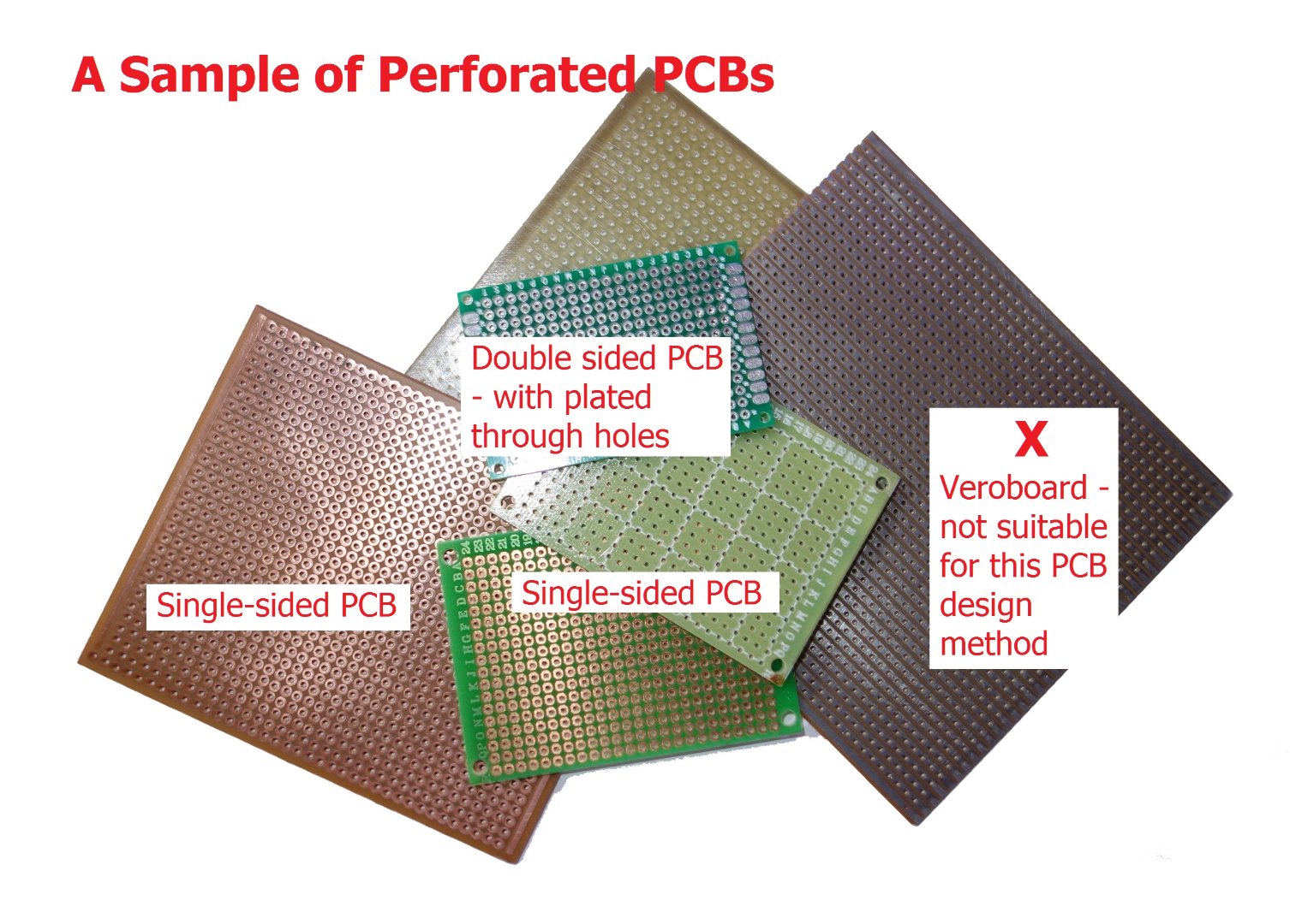
I use both, single sided PCB with a pad for each hole and double-sided PCBs with pads on both sides and plated through holes ... Sample pictures follow.
Just a word of caution here: If you are looking for a complete reference on how to use Cadsoft Eagle, you are in the wrong place. The way I use it is not the way it was intended to be used. I just found this the easy (lazy, fun) way and I am sure you will too if you are only interested in getting your PCB done ... No need to go through the trouble of learning the intricacies of the app :)
If you are interested in doing it the right way, the documentation is available here.
There is also a guided tour here and lots of YouTube videos available.
Downloading and Installing Cadsoft Eagle

Cadsoft Eagle (we'll call it "Eagle") is not freeware, but you are given the option of chosing the free or Light Edition during the installation.
You can read about the Light Edition limitations here. The main concern may be the board size limitation (100mm x 80mm (4" x 3.2")), but because my PCBs are so compact, this has never been a limitation for me. In fact I have even designed two small boards on one sheet.
You will be happy to know that Eagle is available in every OS. You can download it here (screen shot above).
If you use Linux, it is also available from the Software Centre.
Installation is very easy.
As mentioned previously, towards the end of the installation you are offered the License options. If you want to use it free forever as a student or hobby user, with the limitations mentioned, select "Run as Freeware" .
The Guidelines


_Mod.jpg)
Basic Guidelines for Designing a PCB My Way
In order to make my designs manageable, I follow a few simple guidelines:
- This design method is suitable for all kinds of 0.1" perfboard except Veroboard (see the samples in the first picture).
- All designing is done from the point of view of the component side i.e. you are "looking through" the board to see the interconnecting tracks; and IC pin numbers are counter-clockwise. This is set by Eagle.
- All components and wire tracks should be laid out in a 0.1" grid. You can, of course, ignore this guideline and have tracks between holes, but this makes fault finding more difficult.
- You can only use ICs and connectors with a 0.1" pin spacing, though I have made perfboard designs for pentawatt configuration power ICs by offsetting the pins.
- To reduce wiring errors and make circuit tracing and fault finding easier, as much as possible, try to place all resistors and capacitors parallel to each other.
- Jumper wires can be added in the same way as you would add tracks to the component side of a double sided PCB.
- Since we may use bare wire for the jumpers, components should not be placed over them. If it can't be helped, it's best to use insulation tape over the jumper while assembling the PCB.
- To avoid the possibility of accidental short circuit, resistors/capacitors are never mounted vertically (it also looks ugly!).
- The final design should not only be functional but should look good (See the attached sample ... both sides ... For anyone interested that's a Zombie Chorus guitar effects board (the schematic included is from a Russian website). You won't find this size or smaller PCB anywhere).
Note: These are my own guidelines that help me achieve the results that I want i.e. professional looking functional PCBs that are easy to fault-find or modify. Each of you will have your own goals and will eventually make your own guidelines, but for a start, you need to have something. You can freely use mine.
Last and most important of all is: Never wire components together for a project without a PCB design (even if it's drawn on a scrap of paper). The reasons are many, but the most important is that if anything goes wrong or if you want to improve on the design, you have no reference to how you wired up the components besides the circuit diagram (schematic). You have a long and tedious task ahead.
Getting Started
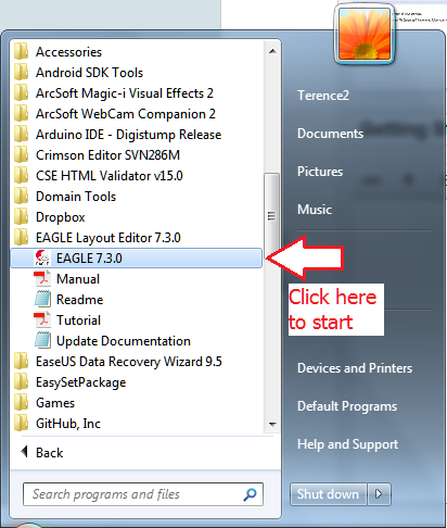


Start up Eagle and create a New Project as shown in the first two pictures.
Name the project folder with the project name.
For this Instructable I am going to use one of my previous designs for the smallest size LM386 amplifier PCB that I could make, so we will name the project LM386 Amplifier.
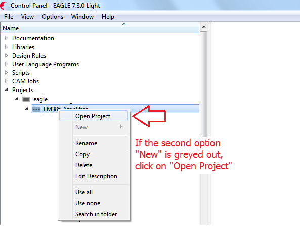
Next right-click on the LM386 Amplifier folder and follow the instructions in the third and fourth pictures.
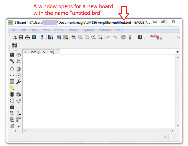
The window on which you will do the actual design opens up (picture five).
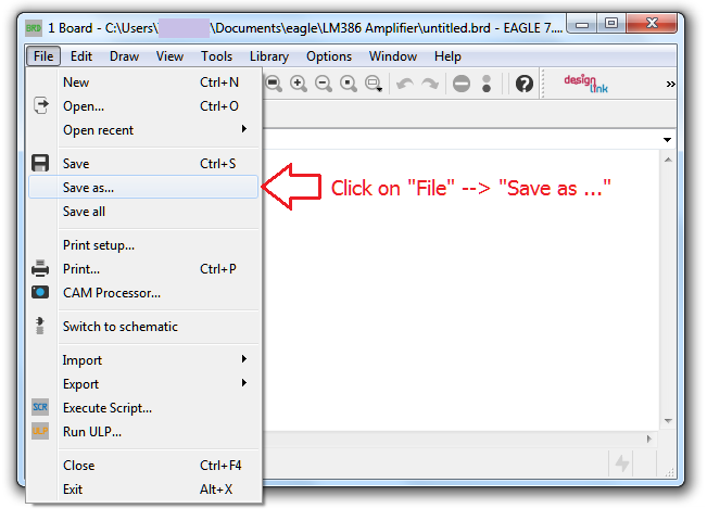
Follow the instructions in pictures six and seven to rename the file LM386 Amplifier.brd and save.
Setting Up the Design Environment

We now setup the design environment in the window we just opened and renamed.
Follow the instructions in the picture for changing the grid to 0.1" and making it visible. This is an important part of getting the component placement right.
In the second of the two screens in the picture, you should see the grid, but the resolution may be too low. For a clearer view, click on the picture and select ORIGINAL(1766x682).
We will now proceed with the library setup. You only need to do this only once. This setting will be saved.
Setting Up the Library


The first thing we have to do before doing the actual layout is to place all the required components on the design board. Everything that we need is stored in Libraries.
When you click on the Add button shown in the picture, a list of library names should come up. Clicking on the arrow on the left of the Library name then drops down the list of the components within, from which you can choose what you need for your layout.
If there are no names in the Library window, it means that your Library has not yet been set up. It's very simple to set up the library. Please follow the instructions in the second picture.
You have to give it some time to populate the design database.
When the Library update is completed, you will see all the Library folders when you click on Add.
We are now ready to populate the design board with the components needed based on your schematic.
Explanation of Some of the Icons
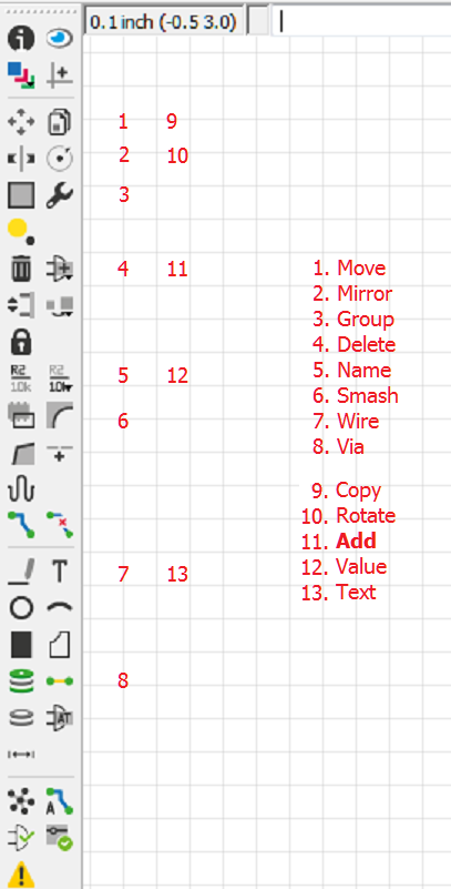
Before we start with the actual designing, it is probably best that you know the functions of some of the symbols in the panel at the left of the PCB design screen.
Explaining them all will take up one whole Instructable on its own, so I am only explaining the few that you will need to carry out the operations for my manual method for making PCBs.
Please explore the other functions as and when you need them.
You don't want to go back and forth to this Instructable every time you are making a PCB, so I have made a separate PDF file with everything you need. Make a printout and have it handy for quick reference when you are actually making your PCB.
This should cover everything you need to get started.
Downloads
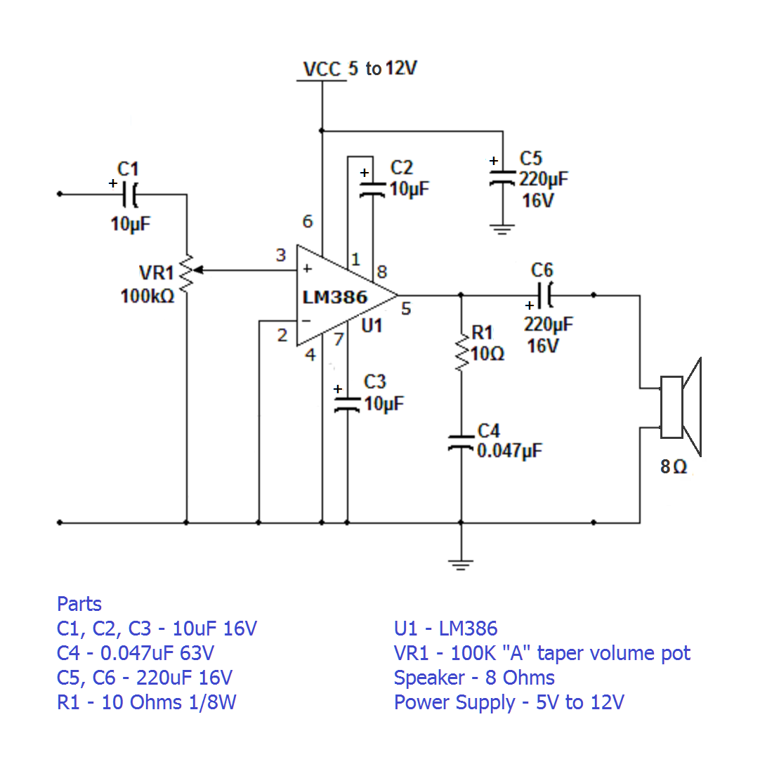
The Circuit Diagram (Schematic)
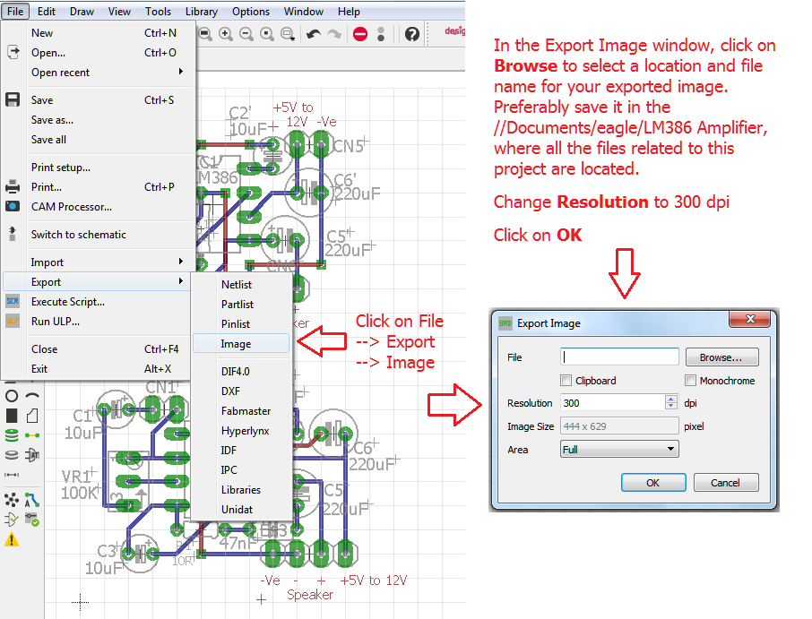
The latest versions of Eagle allow you to save picture files e.g. .JPG, .PNG or even .PDF within the project folder.
You are also allowed to see, double-click and open these files in their own viewers from the start screen of Eagle (the older versions didn't allow this).
For this PCB layout demo, we are going to use the above LM386 circuit (which is available all over the web ... not sure who the author is). I have added in the component values so that it is easier to cross-reference while designing the PCB.
We will not be redrawing this circuit in Eagle (too much trouble for the lazy!). We will just open it side by side with the Eagle PCB layout screen for reference while we make the PCB manually .... I told you it would be fun :)
Download this file and save it in the folder ... //Documents/eagle/LM386 Amplifier, which you just created.
When you start up Eagle and open the folder Projects/eagle/LM386 Amplifier, you will see this .PNG file. If you double-click on it will open in its default picture viewer (not in Eagle).
Component Selection


So far, we have:
- Set up our Project folder
- Set up the work environment
- Named our PCB design
- Set up the components Library
- Studied a few of the symbols that we will work with.
- Selected our Circuit (schematic)
Don't you think it is about time we started actually making our PCB?
Here we go!
- Open up the Eagle application.
- Click on the arrow to the left of Projects, then eagle, then LM386 Amplifier.
- If you followed the instructions so far, there should be only two files. A .BRD file and a .PNG file.
- Double-click on each of them to open them.
- Stretch them vertically and place them side by side as shown in the first picture above.
Next, click on Add to open the Library so that we can select the components that we need (see the first picture).
I have attached a table (second picture) to show you which Libraries I used and which components I selected from each Library. The listed Libraries contain components that you will use for most PCB designs, audio as well as digital, so you can save this table as a guide for future PCB designs. Explore other Libraries, download custom ones or make your own as you become more familiar with Eagle.
All the component selection is now completed. Here is a short note regarding the components I selected:
- VR1: I couldn't find a component to match the green pot on my PCB, so I used a preset with the same pin spacing instead. I previously confirmed the actual space required by the pot on the PCB.
- Pin Headers: You will know from the schematic how many external connections you will need, but at this stage, you won't know how you are going to design them in. I made this PCB before, so I included the pin headers for ease of explanation. In your own design you will be adding them in towards the end.
- Component size: The sizes for most components e.g. ICs, transistors, resistors, pin headers are fixed. Only capacitor sizes vary. I look for the smallest size with the same or higher ratings. I also physically check on the perfboard to see how much space each type needs, so I know which outline to choose from the library.
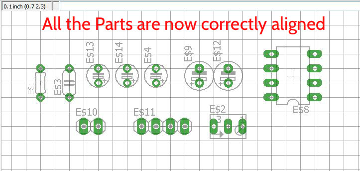
- Repositioning components to the 0.1" grid: In order to connect one component to the other, their connecting points should correspond to the crossing points of the horizontal and vertical lines of the grid. However when you pick them from the library, their leads may not always correspond to the grid as required. For pictures 4 to 7, I have made the grid lines darker so that you can see what I mean. Please follow the instructions in those pictures to correct the position of the components. There are other ways of doing this, but this is the easiest. Unfortunately you have to do each one individually ... no shortcut!
The PCB Design

The actual PCB design is entirely up to you and your imagination. It is more of an art than a science.
Follow The Guidelines and you can't go wrong.
Laying out the Components
When you are selecting your components from the library, make sure that you have picked exactly the same number as in the schematic.
For beginners, at this stage, it would be a good idea to Smash each component, enter the Name and Value of each and reposition the Name and Value using Move (Left-click to move; Right-click to rotate) for easy viewing. This this will confirm that you have all the required parts at the start of the design.
Positioning and Interconnecting the Components
Position the biggest component first. In this case it is the IC. Always rechecking with the schematic beside the the PCB design window, follow up with the components that are nearest to the IC pins.
Use Move to move components, right-click to rotate 90deg, Wire to link them together, Delete if you make a mistake or you are redrawing a line in a different position, Undo or Redo when necessary, Esc if you start a function (e.g. drawing a wire) and you realise that that's not what you want to do and add Vias if you need to have a jumper on top of the board. Change to red Wire for jumpers. Try to keep the jumpers under the IC, so that they take less PCB space.
Checking your Interconnections
Using my LM386 Amplifier as an example, after you have made a few connections, referring to the schematic recheck the connections you have already made e.g. at pin 1 of the IC there is only one capacitor. The +ve goes to pin 1 and the -ve goes to pin 8. Check that this is correct on your PCB layout ... Next pin 2 and pin 4 go to ground along with ... etc. Check each pin, 1 to 8 irrespective of whether it is only connected to another pin which you checked earlier e.g. when you get to pin 8 recheck that it is only connected to pin 1 and nowhere else. Catching a mistake early can save a lot of time and trouble fault-finding later.
An Overview of PCB design
Your first design will never be your best, but practice makes perfect.
A good example is the LM386 PCB that I based this Instructable on. After designing and wiring the PCB (as shown in my intro picture), I was not too happy with fact that the resistor is wired over a jumper and the filter capacitor lead is wired between holes, so I decided to have another go.
I grouped the complete old PCB design (using the Group symbol), and using Copy, made a duplicate of it above the original. Then referring to the original layout and the schematic I redrew the PCB. There is a lot of space under the IC, so the resistor went there. I selected a bigger size resistor from the Library so that I could wire two tracks between its connections. I used three 2-pin headers instead of a 2-pin and 4-pin ... Finally ending up with a a PCB that is one row of holes shorter than the original ... one of my design goals "as small as possible"!
You can see the original and new design in the picture above.
Guidelines for Wiring the PCB


Now that your PCB layout is checked, re-checked and confirmed ready, you can quickly and easily wire it up on a perfboard. Here is an easy trick to ensure that your PCB will be wired error free.
Making an Image File: Open up your PCB design and follow the instructions in the first picture to create an image of it. The image will have the .PNG extension by default. Don't change it.
Making a mirror image of the original image: In this step I am using MSPaint because I find it the easiest for this job. I will explain what needs to be done in Paint, but you can use any other similar application that you are fimiliar with.
- Open up your image file in Paint.
- Select the whole picture ... Ctrl-A (The second picture above shows what a selected image looks like in Paint).
- Copy the whole picture ... Ctrl-C.
- Deselect the picture by clicking anywhere outside the selected area. The copied image will remain on the Clipboard.
- Click and hold the little square at the right-center of the image and drag until the canvas is slightly more than twice its width (see the third picture above) .
- Paste the image that you just copied ... Ctrl-V. It will appear as selected exactly over the original image.
- Keeping the new image selected, go to Rotate in the Paint menu and select Flip Horizontal. The image will be inverted. If you have only one PCB design you can also flip-vertical if you prefer.
- Still keeping it selected, use the keyboard Right Arrow to move it all the way across to the new space that you just created.
- Save the image.
You now have two views of each PCB design on one sheet ... The top of each PCB (the component side) and the bottom (the wiring side) ... See the fourth picture above ... You now know exactly how the Parts will be laid out on the top of the PCB and how the wiring will look when you flip it over. You can't go wrong with the wiring now!
The component Name/Value in the inverted view will be inverted, but still readable. If you are a stickler for perfection and you have a lot of time on your hands you can correct each Name/Value by selecting it using Select and flipping it using Flip Horizontal. Depending on how you positioned the Name/Value, not all can be flipped without some additional work. Believe me. I tried it!
You will most likely decide to wire the new design. I have left the original one as a reference if anyone is interested. You can easily crop it off in Paint by dragging the little square at the bottom-centre of the image upwards till original design disappears before saving. In Paint, cropping only works when the image is de-selected.
Some of My PCB Design Examples


Finally, here are some samples of some of the PCBs I am working on (first picture). Some still need completion and a casing, others I just made for test use.
Notes on Wiring Your PCBs
Here are some additional notes on wiring the PCB:
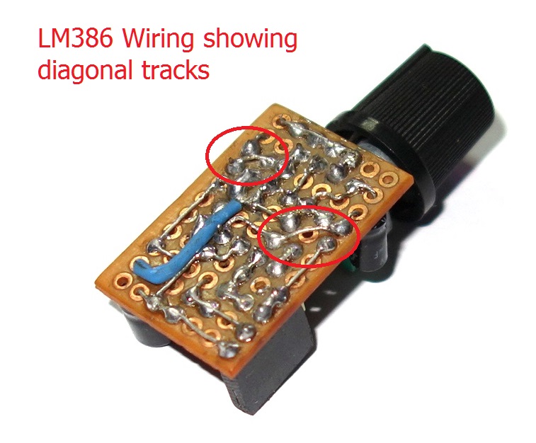
Wiring the Tracks: Use the component wires and component wire off-cuts for making tracks; and single strand hook-up wire for longer tracks
Diagonal Tracks: See the above second and third picture for a sample of how to wire adjacent pad diagonal tracks. For longer diagonal tracks use heat shrink sleeving.
IC Sockets: Use strip sockets cut to size rather than regular IC sockets. There is more space between the rows of pins, and it is easier to solder in jumpers any time during the wiring.
Note on Double sided PCBs with Plated Through Holes: There are some advantages of using double-sided plated through perfboard, but you have to be careful when wiring jumpers, be sure that they are in insulation sleeving. A jumper without insulation over a few holes will short out all the connections below it.
Conclusion
Eagle is a full-function universally accepted PCB design software. There is no limit to the level of PCB design that can be achieved with it. I have taken (and probably misused :)) only one of the features; but you have to admit that it makes it easier for lazy guys like me to make good PCB layouts!
The best part of it is that now that your PCB design is complete you have very little work left (e.g. adding a ground plane, etc.) to make it into a PCB which you can etch if you want to mass produce later.
If you are intending to design complex PCBs for eventually etching (the "regular" way), I found Eagle the easiest and most intuitive software to use.
NOTE: If you are looking at older Eagle tutorials, keep in mind that in the later versions (starting from v7, I think) some of the symbols in the left panel were changed e.g. the Delete symbol changed from an "X" to a waste-bin, the Copy symbol changed from two stick men to double sheet, etc. The older tutorials will still show the old symbols, but the positions are the same.
There is a huge library of designs for free download available on the Eagle homepage. Also, many project designers provide Eagle files for their PCB designs, which you can download and modify, if necessary, to suit your available components.
Avoiding Fault-finding
If you read my text carefully and between the lines, you will see that I place a lot of emphasis on avoiding fault-finding on your wired PCB. This is the repair technician in me. Most hobbyist rush through the PCB design stage and end up spending hours (or days) fault-finding after they have wired the PCB.
I would rather take my time with the PCB design, rechecking the interconnections while designing the PCB and enjoy running the project as soon as it is wired up.
If you like this tutorial and you enjoy PCB designing, why not share some of your designs on Instructables?
Good luck with your PCB designing!