Free KiCad Crosstalk Heatmap Simulation and How to Improve Magnetic Field Emissions With OpenEMS
by Renato Panic in Circuits > Arduino
2154 Views, 8 Favorites, 0 Comments
Free KiCad Crosstalk Heatmap Simulation and How to Improve Magnetic Field Emissions With OpenEMS

Applications like LTSpice are very efficient to verify your schematic, but there are not many tutorials on how to verify your PCB layout efficiently. I will try to fill that gap, starting with this Instructable.
Once you transition from schematic to layout, the parasitic effects (like trace impedance, capacitance, inductance, etc) of your board start to play a significant role. Trace impedance, crosstalk, electromagnetic emission, and other factors cannot be efficiently simulated by just simulating the schematic. This is why once your designs get more complex eventually you will start encountering problems with electromagnetic compatibility (EMC).
EMC issues can lead to numerous problems. Some common examples include:
- The board stops working after you "simply touched it" or moved it slightly (Cause: Electrostatic discharge, or ESD).
- The board has random glitches (Cause: Electromagnetic interference or crosstalk)
In this tutorial, I will show you how to review your PCB layouts crosstalk inbetween traces and the magnetic field emissions around the PCB.
Supplies
The amazing thing about using a simulation is that no physical supplies are needed. But you have to install some free software tools. With free i mean completely free, even for commercial use.
Please download following software tools:
1) KiCad 6.0 - if you are a first time user please use KiCad 6 to avoid any dependency problems
2) FreeCAD - ideally use version 0.19 to avoid any dependency problems
3) openEMS - here is a full tutorial on how to install it: openEMS installation tutorial
4) ParaView - we will use this application to view our simulation results
Prepare Your KiCad Layout

Download the KiCad project from the google drive link.
Download the folder Orginal-PCB, extract the zip file and check if you can open the provided kicad layout.
If you can open the KiCad file as shown in the screenshot, you are ready go to to the next step.

Open Freecad and start the FreeCad to openEMS macro.
If you dont know what that macro is, you did not watch the installation tutorial yet, watch it here.
Import the 3D Model of Your KiCad Layout Into FreeCAD


1) Click on the button "KiCad PCB Import Tool"
2) select the KiCad File and enable the checkmark "Fuse copper ..."
3) Click on "Import KiCad PCB". The import will now take a while, the report view will give you an "all done" message once the import is finished
Prepare the 3D Model for Simulation


As the initial import of the 3D model has a lot of parts and shapes, our goal now is to simplify the objects to just end up with one FR4 object and one copper object. For this you have to perform following steps:
1) Expand the object called "coppers_drilled#F.Cu"
2) place the 2 child-objects outside of their parent object. This is done by copying them and then pasting them outside of their parent-object "coppers_drilled#F.Cu"
3) change to the parts workbench
4) mark the child objects and "Fuse" them
5) create a simple copy of the fused object
6) Now also create a simple copy of the PCB object (objectname is "board_solid")
7) delete all other objects and only keep the 2 simple copies that you created in 5) and 6)
8) create a box
9) call the box air and adjust it so it covers the whole PCB and is 1mm bigger than the PCB in every direction
10) mark all objects and make them 90% transparent so we can see inside the airbox and components.
11) Copy the airbox, call the new object field, change the height to 0.1mm and place it inbetween the top and bottom layer of the PCB. We will use this very thin box to later measure the cross section of the magnetic field inside the PCB.
12) You now can create 2 additional field boxes to additionally measure the magnetic field above and below the PCB.
13) The next step will be to create a small box between the VCC power supply signal and GND.
14) For the Arduino board in our example the size of the small box will be 3x1x0.05mm (0.05mm are 50 micrometers, which is the height of the copper layer).
15) if your desired board has another copper thickness or board thickness, you can simply change the layerstack information within KiCad.
16) now run the "FreeCAD to openEMS" macro again, change to the "Grid Settings" tab and setup the grid as shown in the screenshot
Setup the Simulation Parameters of the FreeCAD to OpenEMS Macro


1) change to the tab "Grid Settings" and setup the grid as shown in the screenshot
2) go to the Tab "Material Settings" and create one additional material called "air" (Epsilon = 1 and Mue = 1)
3) Create another material called FR4 (Epsilon = 4.6 and Mue = 1)
4) change to the tab "Excitation Settings" and create a step function
5) change to the tab "Port Settings" and create an "active" port with 1666V/m and direction in "x"
6) change to the tab "Probe Settings" and add a H field probe. The H field also is called the magnetic field. You could also measure a lot of other fields as for example the electric field or also the current density field or so called J field but for this tutorial we will only measure the H field.
7) change to the tab "Simulation Params" and reduce the timesteps to 20000 and the min decrement to 0.01. All the boundaries have to be set to PML, PML means perfectly matched layer and tries to mimic an extension into infinity.
8) Now change to the tab "Object Assignment" and set up all Object as shown in the screenshot.
9) save the settings file in the same folder as your FreeCAD project. Also make sure that your FreeCAD project is saved by now.
10) Generate the openEMS code via the Button "Generate OpenEMS Files", a popup will open after that which you can confirm with a click on the "ok" button.
Run the OpenEMS Simulation With the Generated Python Script


1) change to the simulation output folder and edit the generated python script (file ending ".py") via a text editor of your choice.
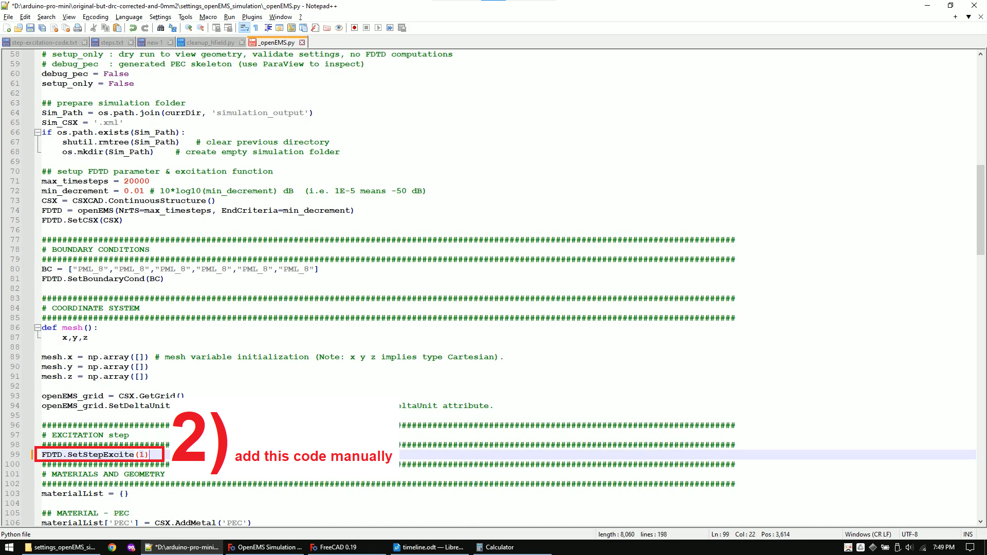
2) The "FreeCAD to openEMS" Macro has a bug here and does not properly generate the code for the step function. Hence we have to add the code manually.
3) Optional step: you can now make the Hfield probe perfectly flat to measure the cross section of the Hfield, but the simulation will run fine also without this step.
4) double click the python script to run the openEMS code. After that a 3D preview of the simulation will popup.
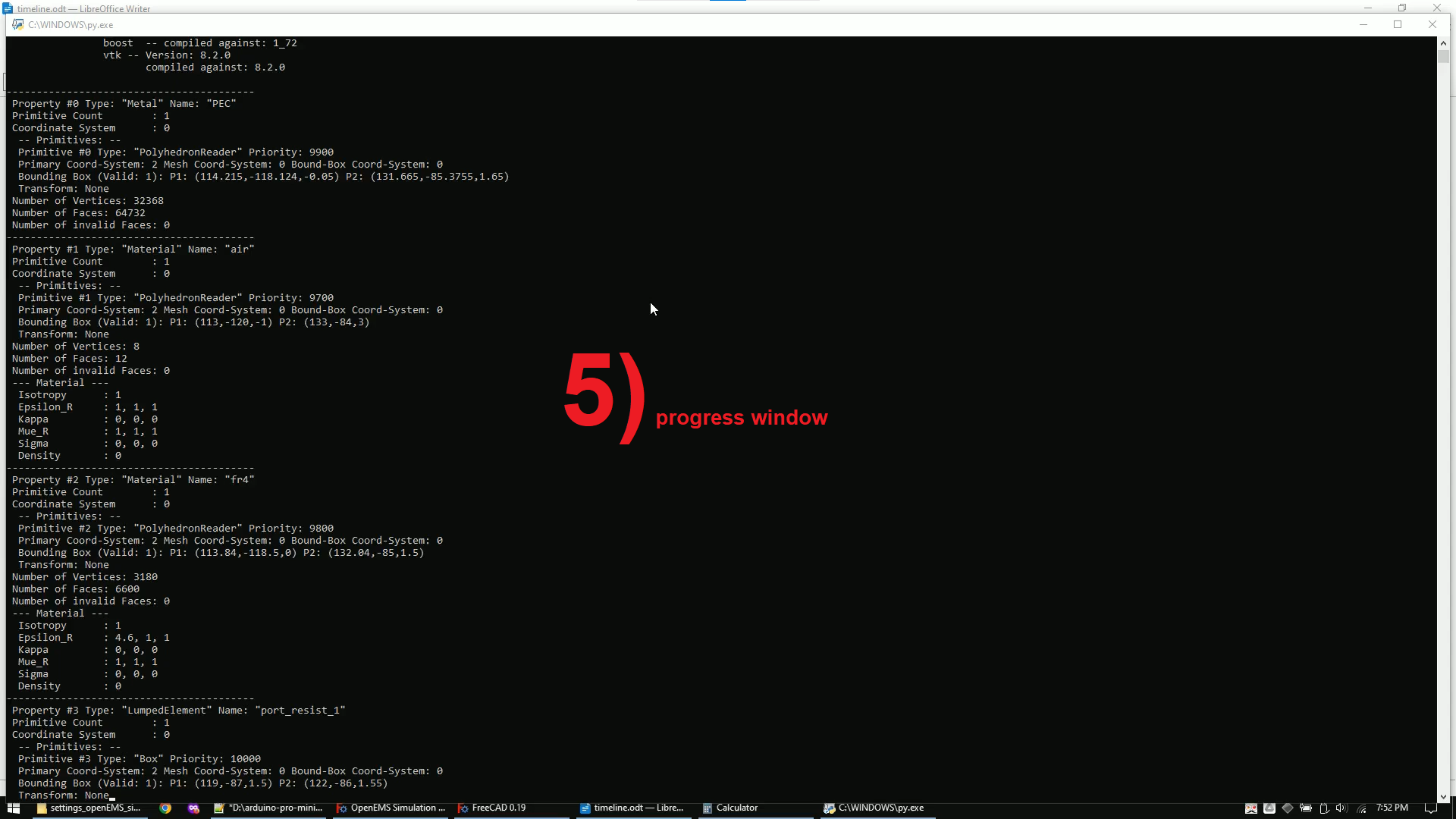
5) Once you close the 3D preview, your simulation will start, the progress will be shown in text format inside the command line window.
View the Simulation Results With ParaView


1) After the first few timesteps were simulated, you can open the output folder. If you type in Paraview into the explorer bar and hit enter, it will open paraview.
2) press open, you should now already be in the correct folder location.
3) now open the vtr-files
4) change the color style to H field
5) you can set the color range with the button that is shown in the screenshot.
6) change to timestep 1000 to see if the color range was set to a suitable value
7) Optional: add the stl file of the copper traces.
8) Optional: make the copper trace layer 1000 times smaller. This is because the stl file was stored in mm, but paraview uses the unit meters.
9) Optional: You can change the color of the copper traces to orange so it looks more like copper.
10) set the opacity of the copper object and the Hfield object to 0.5, so that you can see the traces of both the top layer and bottom layer as well as how the signal propagates through your PCB.
Improve the Magnetic Field Emissions


After you know how to setup the simulation, you can now simply try to reduce the crosstalk of your VCC trace.
You can also repeat this step for all other signal lines that you are interested in. You could also inject a step pulse into every signal line of the PCB at the same time, but then you would not be sure what noise comes from which trace.
A few tips on how to improve the electromagnetic emissions from a 2 layer PCB:
1) Every signal that crosses another signal should have a return current via on all sides. If several signals cross each other, the layout should look like in the screenshot.
2) If just 2 signals cross each other, then place the vias as shown in picture 2 of step 8.
When you look at picture 3, you will see that randomly via stitching a PCB is not really helpful, even though many layout engineers do that. Please keep in mind that layout engineers often are not too experienced regarding EMC - even after decades of work experience - as they typically dont spend time in EMC chamers to troubleshoot problems, they follow layout design guidelines which often come with "strings attached" and might help with one problem but generate problems in other areas.
4) If you dont really know what you are doing (yet), changing from a 2 layer PCB to a 4 layer PCB is a good start as it improves emissions without you having to think about it.
The big advantage of a 4 layer board is that it reduces the distance from GND to the signals on each layer from typically 1.6mm to just 0.2mm which is 8 times less. This increases the capacitive coupling between the traces and GND which reduces the capacitive coupling effects to "the rest of the world" and hence reduces emissions.
Another major advantage advantage is that you automatically eliminate all ground plane interruptions beneath the traces by having a continuous ground plane below all of them.
However, keep in mind that even a 4 layer board with full ground planes on L2 and L3 does not automatically ensure that ground is next to each trace. It also does not address the issue of missing return current vias during layer transitions (see picture 5)