How to Get Schematics Fabricated
by Autodesk Circuits in Circuits > Electronics
25662 Views, 74 Favorites, 0 Comments
How to Get Schematics Fabricated
123D Circuits.io is a site where you can design circuits and PCBs in your browser for free.
This instructable will guide you through all the steps of creating and ordering a PCB.
This instructable will guide you through all the steps of creating and ordering a PCB.
Getting Started: Creating an Account

First you have to create an account at https://123d.circuits.io You can also use Facebook or Twitter to log in.
Creating a New Circuit

On your dashboard, click "New Circuit".
Creating a New Project

Enter a name for your project, select the type of project (choose schematic circuit for this design), and click "Create new".
Circuit Design: the Sidebar
Circuit Design: Adding Components

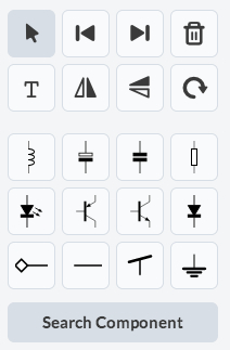
To add common components, you can drag them from the left sidebar. If you need more advanced components, click on the "Search Component" button. Here you'll be able to search for other components. You can append an asterisk (*) to search with prefix wildcards, for example "74HC*".
Another example, if you want to add a screw terminal, search for "connector" and choose one.
Another example, if you want to add a screw terminal, search for "connector" and choose one.
Circuit Design: Component Value

You can give your components a value by clicking on it and filling in the detail in the inspector appearing at the bottom of the screen.
Circuit Design: Connecting Everything

To connect two points with each other:
- hover with your cursor over the component and click on the red square denoting a component terminal,
- click the other point in the schematic you want to connect it to (this can be either an existing wire or a terminal)
- hover with your cursor over the component and click on the red square denoting a component terminal,
- click the other point in the schematic you want to connect it to (this can be either an existing wire or a terminal)
Circuit Design: Using Labels


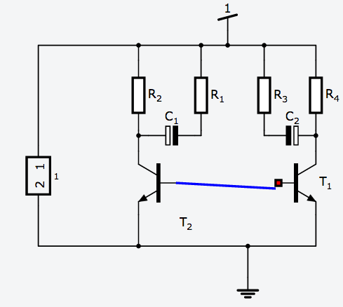
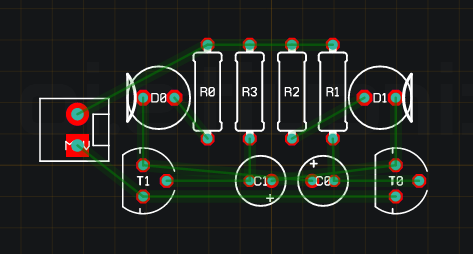
If your schematic is getting more complicated, you can keep it clean by using labels. The schematic on the 3 following screenshots is logically the same.
PCB Design

Now that he schematic is complete we can start designing the PCB. This process is often called "laying out a board" or simply "layout" since it involves laying copper traces on the PCB.
Click in the menubar on the left to go to the PCB design.
Click in the menubar on the left to go to the PCB design.
PCB Design: Sidebar

PCB Design: Footprints

By default all the footprints are small surface mount components (SMD). If you want to change the footprint to through hole or any other package, select the component and choose the a different footprint in the pop-up menu.
PCB Design: Placing Your Components Apart
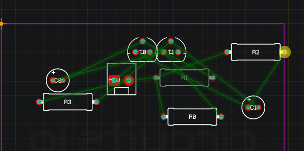
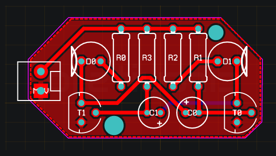
Place your components such that not too many green lines cross and the design will be easily routable.
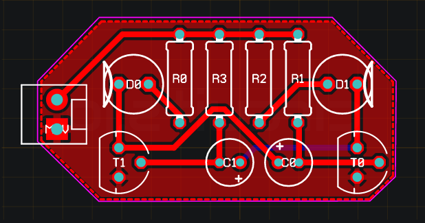
PCB Design: Routing the Paths
The green lines, all together called a "ratsnest", and individually called "air wires" denote the electrical connections that you need to convert to copper traces. These come from the schematic design you made earlier.
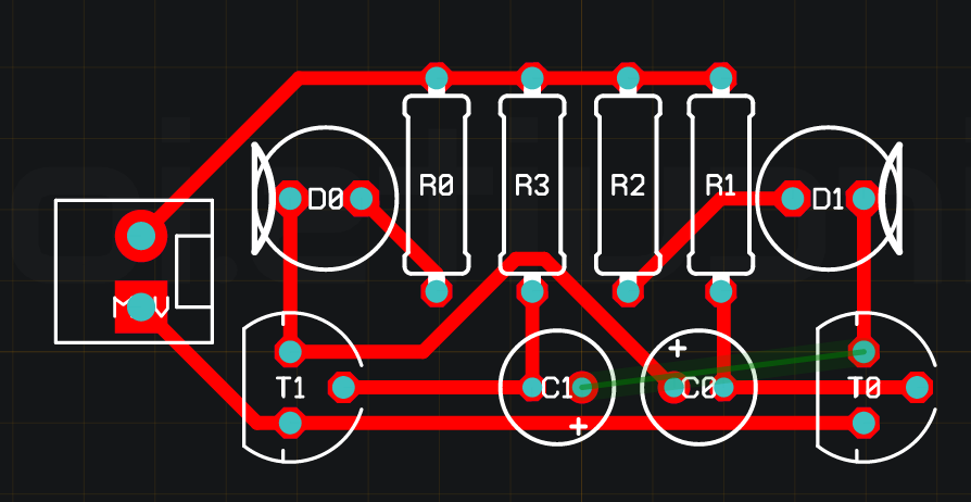
Switch to the routing tool and click a pad to get started. Route the trace by moving your mouse and clicking at intermediate points until you reach the other side of the airwire. Make sure not to cross or come too close to other lines. The tool will show a warning when you make a mistake.
If you're stuck you can switch your trace to the other layer by pressing "L" on the keyboard or change the layer in the select box.
In the screen shot, you can see that for last connection I could:
- Rearrange my components or paths.
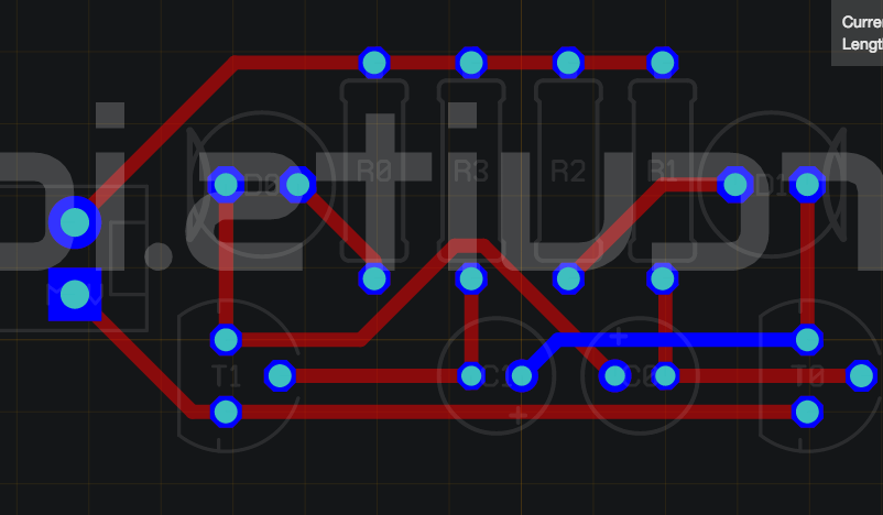
- Route the wire on the other side of the board, which is much easier. Double layer boards are standard on 123D Circuits.io and don't cost extra when ordered. The blue traces are on the bottom side of the PCB.
Switch to the routing tool and click a pad to get started. Route the trace by moving your mouse and clicking at intermediate points until you reach the other side of the airwire. Make sure not to cross or come too close to other lines. The tool will show a warning when you make a mistake.
If you're stuck you can switch your trace to the other layer by pressing "L" on the keyboard or change the layer in the select box.
In the screen shot, you can see that for last connection I could:
- Rearrange my components or paths.
- Route the wire on the other side of the board, which is much easier. Double layer boards are standard on 123D Circuits.io and don't cost extra when ordered. The blue traces are on the bottom side of the PCB.
PCB Design: Adding Polygons

To add a ground plane:
- click on the polygon tool
- click on a wire or pin you want the ground plane to be electrically connected to
- draw a polygon around your components
The polygon tool will be auto-computed to not be connected to any net except the one you originally connected with. Note that the copper pour is auto updated when moving components. Regions where the copper could not be electrically connected will not be filled with copper to avoid "floating copper" which can lead to interference.
PCB Design: Reshape Your PCB
You can change the borders of your pcb by clicking on the pink lines around your PCB. You can drag the lines themselves, or click on a blue handles and move them separately. Double-clicking the outline will create a new handle to allow for more complex shapes. When you double clicking a handle, you turn the point into a B-Spline controlled point, allowing crazy bend shapes.
PCB Design: Add Milling Holes
You could add some mounting holes using the drill tool. To change their diameter select it and change the diameter in the pop-up box.
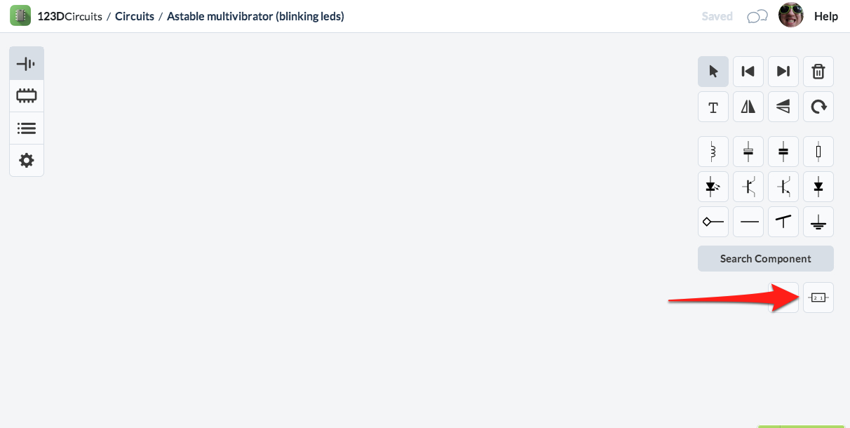
Project Page

If you're done with layout you can now go to the project page by clicking on the name of your circuit. Your circuit layout will auto-save.
Project Overview

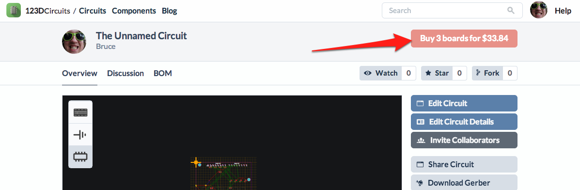
When all the traces are routed go back to the project overview and click "Mark as done". Now the design will show up in the gallery and other people can see it. It is now also possible to order the board.
I you want to order your boards click on "Buy 3 boards for..." Fill in your order details and you will receive high quality PCBs in about two weeks. With free shipping world wide!
I you want to order your boards click on "Buy 3 boards for..." Fill in your order details and you will receive high quality PCBs in about two weeks. With free shipping world wide!
Order Your PCB
Now you can order your PCB by clicking the Buy button.