How to Inspect PCB Gerber Files in 3D Directly in Your Browser
by DavidParry in Circuits > Tools
25 Views, 0 Favorites, 0 Comments
How to Inspect PCB Gerber Files in 3D Directly in Your Browser
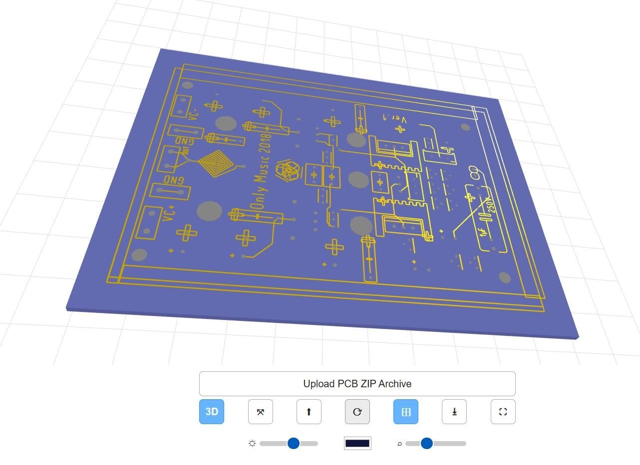
Before sending a Printed Circuit Board (PCB) design off to a manufacturer, verifying the Gerber files is a critical final step. A single misplaced via, an overlapping silkscreen, or a missing copper trace can ruin an entire production run. However, downloading and installing heavy, complex desktop CAD software just to quickly view a design can be incredibly frustrating.
This guide will show you how to use our free 3D Gerber Viewer to instantly inspect your manufacturing files. We will walk through how to upload your designs, manipulate the 3D board, isolate specific layers for debugging, and customize the visual output for client presentations or documentation.
Because the entire process runs locally in your web browser, your intellectual property remains completely secure. Your files are never uploaded to an external server. Let's get started!
Gather Your Files (Supported Formats)
To use this viewer, you don't need any special hardware or software installations—just a modern web browser and your exported PCB manufacturing files.
The viewer is designed to read standard RS-274X Gerber formats and Excellon drill files. You can drag and drop a compressed .zip archive containing your entire project, or you can upload individual files.
The service officially supports and automatically parses the following file extensions:
- Copper Layers: .gtl (Top Copper), .gbl (Bottom Copper)
- Solder Masks: .gts (Top Solder Mask), .gbs (Bottom Solder Mask)
- Silkscreens: .gto (Top Silkscreen), .gbo (Bottom Silkscreen)
- Board Outline / Edge Cuts: .gko, .gm1
- Drill Files: .drl, .txt, .xln
- General Gerber Extensions: .gbr, .gerber, .pho
If your Electronic Design Automation (EDA) software outputs these extensions, simply pack them into a .zip folder and you are ready for the next step.
Upload and Switch to 3D Mode
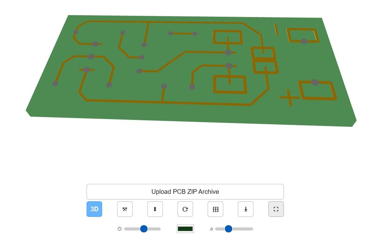
Loading your design is practically instantaneous because all decompression and rendering are handled by your computer's local hardware.
- Upload the Archive: Open the viewer in your browser and either click the "Upload PCB ZIP Archive" button in the top menu or directly drag and drop your .zip file into the main viewing area.
- Initial Parsing: The system will immediately read the text data inside the files, calculate the board dimensions, and map out every trace, pad, and via.
- 2D vs. 3D Mode: By default, you might see a 2D orthographic projection. Click the 3D / 2D toggle button in the top navigation bar to switch to a fully extruded, three-dimensional view. The 3D mode adds physical depth to the substrate, elevates the copper traces, and punches actual cylindrical holes through the board where your drill files dictate.
Navigating and Inspecting the Board
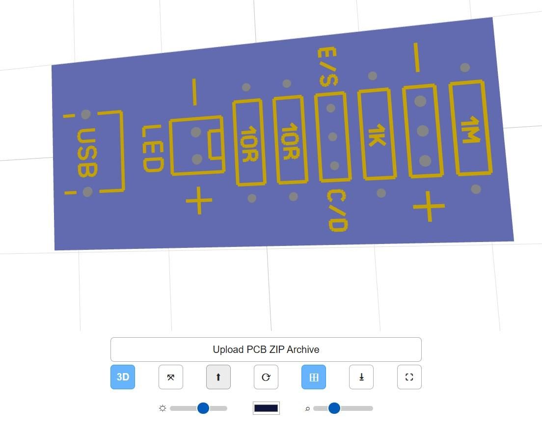
Body Text: Once the 3D model is generated, you have complete spatial control to inspect every millimeter of your hardware design.
- Orbit and Pan: Click and drag to rotate the board 360 degrees in any direction. Right-click and drag to pan across the surface of the PCB. This is crucial for checking alignment between top and bottom layers.
- Zoom: Use your mouse wheel (or the zoom slider in the bottom control panel) to zoom in on high-density areas, such as fine-pitch microcontroller footprints or complex routing junctions.
- Auto-Rotate: If you need to present the board or simply want to view it from all angles without interacting, click the ⟳ (Auto-Rotate) button to set the board spinning on its Z-axis.
- Dimension Grid: Toggle the ⊞ (Grid) button to overlay a scale grid beneath the board. This helps you visually confirm that your overall board dimensions and coordinate exports are correctly scaled.
Layer Isolation for Easy Debugging
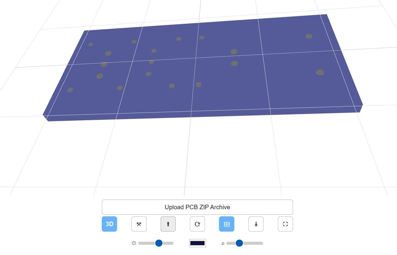
When viewing a dense, multi-layer board, it can be difficult to trace a specific signal path due to visual clutter. The viewer includes a quick layer toggle to strip away the noise.
Click the ⬍ (Toggle Layers) button in the top menu to cycle through visibility states:
- All Layers: Shows the complete board, including the substrate, top copper, bottom copper, and drill holes.
- Top Layer Only: Hides the bottom copper and substrate, allowing you to clearly follow the top routing.
- Bottom Layer Only: Hides the top copper and substrate, giving you an unobstructed view of the bottom traces.
This tool is highly effective for verifying that thermal reliefs are correctly applied and that vias are cleanly connected to their intended traces on specific layers.
Customizing the Look and Exporting
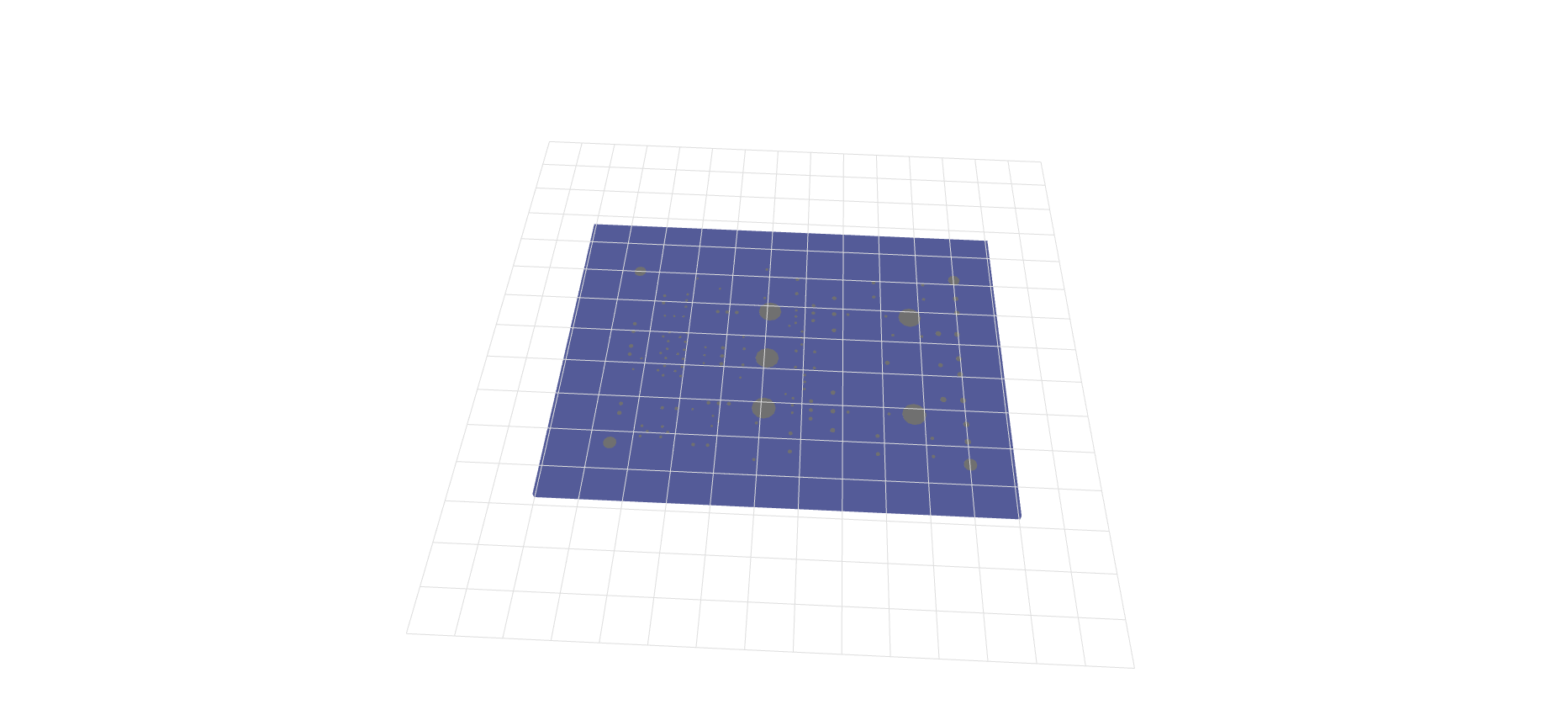
Whether you need high-quality images for a datasheet, a portfolio, or to show a client exactly what the manufactured board will look like, the bottom control bar allows for deep visual customization.
- Solder Mask Color: Click the color picker at the bottom center of the screen. You can change the board substrate from the default dark green to literally any hex color. Testing out how your design looks in black, blue, purple, or white is instant.
- Lighting Control: Adjust the ambient light intensity slider to brighten the scene or create harsher shadows, which helps emphasize the height of the copper traces.
- Save a Screenshot: Once you have the perfect angle and color, click the ⭳ (Download) button. The viewer will instantly generate and download a clean, high-resolution PNG image of the canvas, free of any UI elements.