How to Use the Internal PS3 Memory Card Reader As a USB Device on You PC
15385 Views, 25 Favorites, 0 Comments
How to Use the Internal PS3 Memory Card Reader As a USB Device on You PC


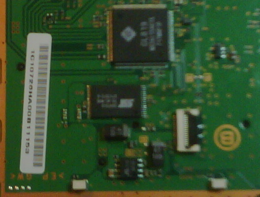


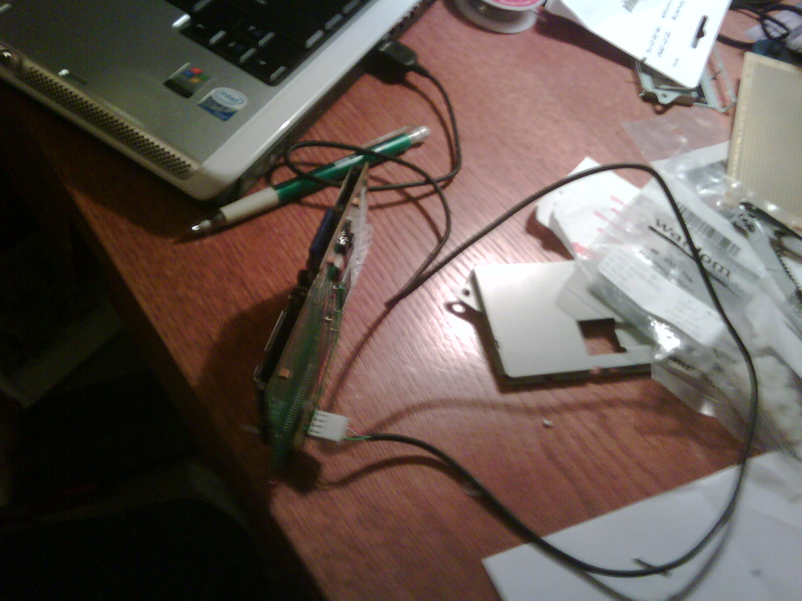


First off this is my first Instructable (yippie!), I'm sure there will be plenty to come.
So, I had a broken PS3 and wanted to make some use of the working components. First thing I did was pull the data sheet for the converter chip on the PS3 card reader. It can be found here
http://pdf1.alldatasheet.com/datasheet-pdf/view/207048/GENESYS/GL819.html
if your not to good or out of practice with soldering, I suggest you don't try this project.
Pulling Apart the Reader


There are 2 metal "mounts" that in-case the reader board.
Remove the top by pulling up at the back of the cover.
The bottom holds the board in place by 2 clip on the sides, just depress them and remove the board.
Remove the top by pulling up at the back of the cover.
The bottom holds the board in place by 2 clip on the sides, just depress them and remove the board.
Map Connections

Next we will need to map out the connections
On the back of the board, you'll notice the ps3 ribbon cable adaptor, here is the pin-out starting from the bottom up, on the picture.
1 - AGND - Analog Ground
2 - DGND - Digital Ground
3 - AGND - Analog Ground
4 - Vcc - Input Voltage 5V
5 - Vcc - Input Voltage 5V
6 - Vcc - Input Voltage 5V
7 - Vcc - Input Voltage 5V
8 - AGND - Analog Ground
9 - EXTRSTZ - External Reset
10 - AGND - Analog Ground
11 - AGND - Analog Ground
12 - USB D- - USB Data-
13 - USB D+ - USB Data+
14 - AGND - Analog Ground
15 - AGND - Analog Ground
Soldering the Connections


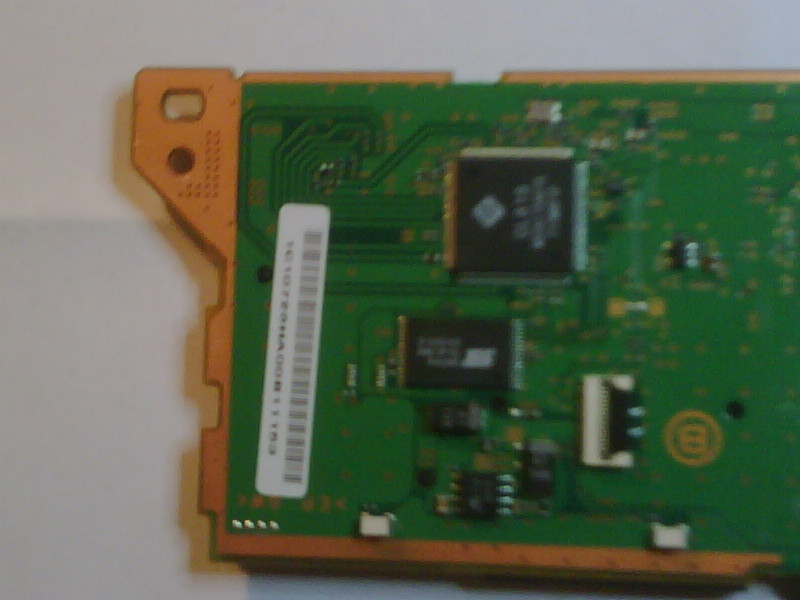
Unless your a god, or have some REALLY nice soldering equipment, you won't be able to solder directly off of the 15 pin connector, so we will have to find alternatives. Even taking a picture of the locations I used, seemed difficult. so I will try to explain.
Pin1 and pin15, analog ground, can be wired directly off of the 15pin connector, they have large contact points and are on top and bottom. This also takes care of Pin3,Pin10,Pin11,and Pin14
Pin4-pin7 are all vcc ,5 volt input, and can be connected to at a solder point directly to the left of the smaller "B" symbol next to the large 4716b diode(red wire).
Pin8 is another analog ground, this one needs to be connect to the GND side of one of the surface mount diodes to the right of the SST39VF010 chip.
Pin 9 does not need to be used.
Pin 12 and Pin 13, the -+USB data need to be connected to lower contact of the resistors directly above the 15 pin clip. NEG- is on the left, POS+ on the right.
And finally Pin2, the DGND. (The problem child) this *should be connected back directly from the 15 pin connector to its own* ground, but I was unable to solder a wire from the 15pin directly, so I soldered pin 2 to pin 1.
Now I know some of you who have dealt with AGND and DGND will tell me that I'm putting digital interference onto the analog ground plane. However, let me remind you, the bus speed this chip runs at does not cause any issues.(that I have found with an oscilloscope)
Connect Wire to a USB Pinout Connector


Here is the pin-out for USB
1 VCC Red +5 VDC
2 D- White Data -
3 D+ Green Data +
4 GND Black Ground
Connect Pin5-Pin7 from the board to USB Pin1
Connect Pin12 from the board to USB Pin2
Connect Pin13 from the board to USB Pin3
Connect Pin1, Pin8, and Pin15 from the board to USB Pin4
You can set this up anyway you would like, but I decided to use a spare piece of pcb board and attach it using some plastic screws to a standard 4 pin USB connector.
I then disassembled a spare USB cable and attached a connector to it, I recommend this, as connecting a usb cable directly the the pcb, probably won't hold up for more than a couple of uses.
Testing


Test you connections! with a multimeter
Make sure you do not have anything crossed, you can blow out your USB port if you do. (No this did not happen to me)
After you have checked everything plug it in. Windows will automatically recognize it as 3 external devices.
Test out some memory cards (make sure they are backed up), nope not me again. :-P
Altering the Metal Brackett


Next we need to alter the metal bracket to allow room for the new connector.
Bust out the dremel and start cutting, hopefully you can do a better job than me. I was excited and over-cut :-(
Thats it, Please leave a comment and let me know what you think.
Bust out the dremel and start cutting, hopefully you can do a better job than me. I was excited and over-cut :-(
Thats it, Please leave a comment and let me know what you think.