Internet-Week Clock


Greetings everyone and welcome back. Here's something fun and helpful.
The Week Watch is a compact desk clock that displays the current day of the week. It achieves this by connecting to a local Wi-Fi network and synchronizing time through an NTP client. Each of the seven LED segments is dedicated to a specific day, lighting up accordingly.
Here, we've changed the code from our previous project (Happy Week Indicator) to create a Week Clock Setup that tells us which day it is by lighting up one of seven LED segments. In this project, we used two PCBs: one for the driver and the other the Art PCB with the name Days etched into the top layer. We created openings in the top and bottom solder mask layers to allow light to pass through the PCB.
The goal was to design a little desk clock that tells us what day it is.
Here, we're using a completely customized LED driver board, each with three LEDs connected in parallel and driven by a Mosfet IC, which is controlled by the DFRobot's Mini Beetle ESP32-C3. To represent seven days, we used a total of seven LED setups, each having three LEDs connected in parallel with a mosfet IC arrangement.
We also integrated an onboard power source, a 2200mAh 3.7V lithium-ion battery, which powers this arrangement and can be recharged once discharged.
This Instructables covers the whole build process of this project, so let's get started with the build.
Supplies
These are the materials used in this project:
- Custom PCBs (Provided by HQ NextPCB)
- DFMini beetle ESP32-C3 Development Board
- IP5306 Power Management IC
- 10uF capacitors
- 10uH SMD inductor
- Blue LEDs 0805 Package
- 8205S Mosfet IC
- 10K resistors
- 3D Printed Parts
- M2 Screws
CAD MODEL


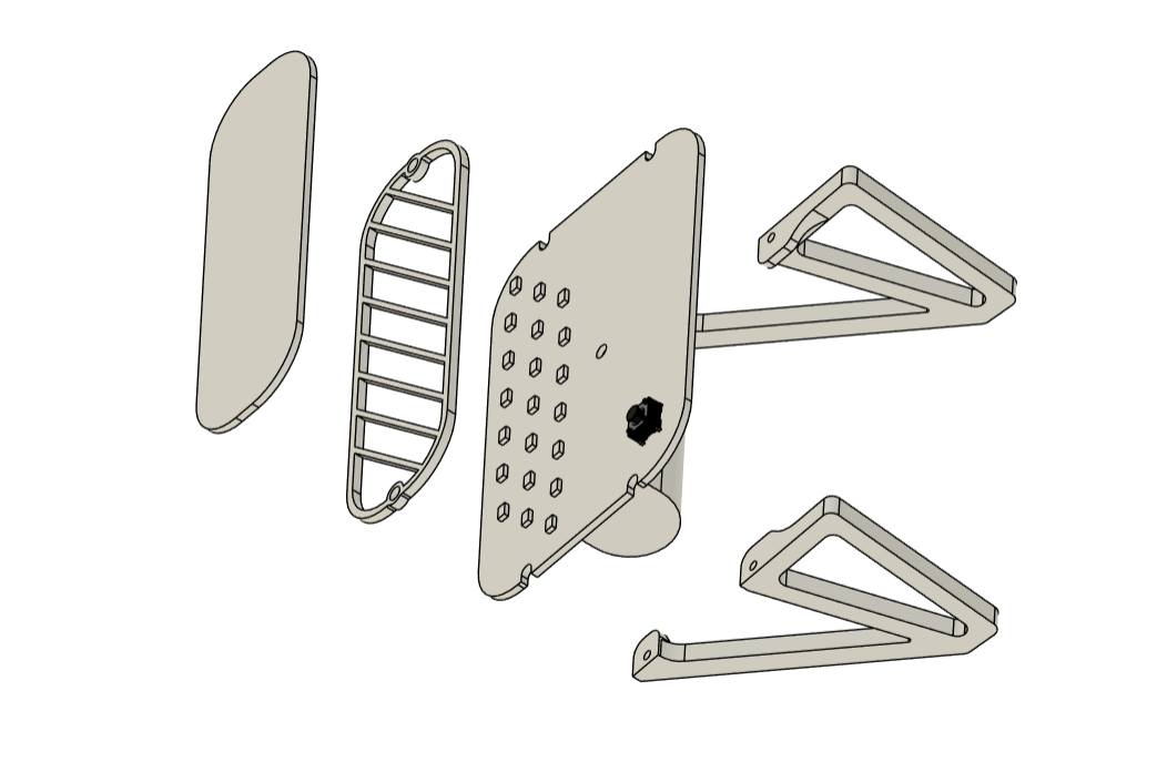
We begin this project by creating a Cad design that consists of a PCB with all SMD LEDs on the top side arranged in a sequence of seven. We place them slightly inclined to achieve the angled effect we want.
The lithium cell as well as the microcontroller and main throughhole components are all modeled on the bottom side.
We also created two stand-like components to help the clock stand in its proper orientation.
LEDs are mounted on the base or driver board, but their glow is seen on another board that is positioned above the LEDs. This is achieved by utilizing a separator part that creates space between the LEDs and both PCBs.
This design requires three 3D-printed pats, all of which were created using black PLA and a 0.6mm nozzle.
PCB Design


We begin the PCB construction process by creating schematics for the project.
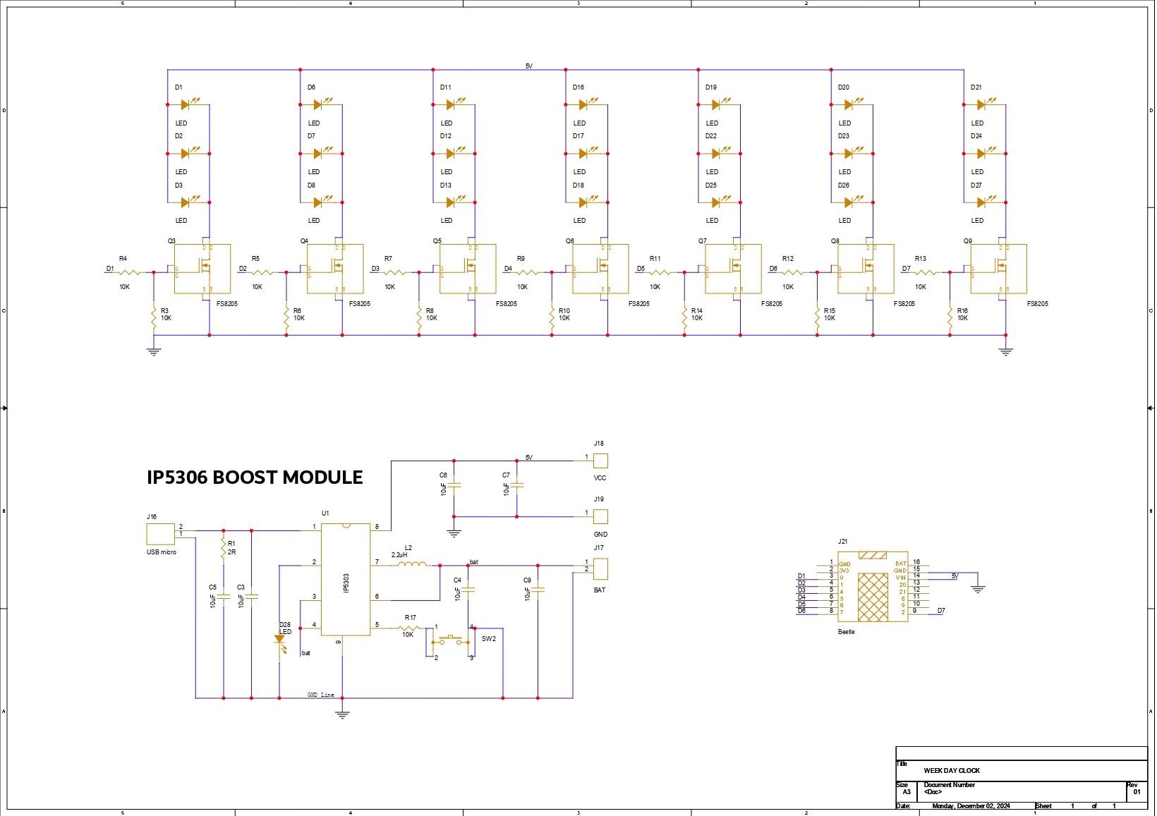
The schematic is divided into three primary parts. The first is the Power Section, which includes an IP5306 Power Management IC configured according to the example layout provided in the datasheet. This power management setup gives a consistent 5V output that our microcontroller and Mosfet IC will use to power LEDs.
The second section is the LED array. We connected three LEDs in parallel and connected them to an 8205S Mosfet IC whose gate is connected to the microcontroller's I/O port via a 10K resistor. An additional 10K resistor is put between the MOSFET gate and source. This design contains seven LED mosfets, each of which is coupled to a microcontroller I/O pin.
The last section is the DFRobot's Mini Beetle ESP32-C3 Microcontroller board, which is connected to the IP5306's 5V and GND outputs, as well as the gates of each mosfet.
Using the cad layout for the PCB, we then prepare the PCB design for this project, which includes the actual placement of the LEDs. Because we will be putting an additional board over the driver board, LED placement is critical, so we use dimensions from the cad file to prepare the PCB and place components correctly.
We also prepare the Art PCB, which is a half-board with no components and only two mounting holes. We also use the cad file measurements to open the soldermask top and bottom on this art PCB, and we place the names of the days on the TOP layer.
After finalizing both PCBs, we exported the gerber data, which will be sent to a PCB manufacturer for samples.
NextPCB PCB Service


After completing the PCB design, we send both Gerber data to HQ NextPCB for samples.
Gerber Data was sent to HQ NextPCB, and two orders were placed: one for the green solder mask with white silkscreen and another for the white solder mask with black silkscreen.
After placing the order, the PCBs were received within a week, and the PCB quality was pretty great.
In addition, I have to bring in HQDFM to you, which helped me a lot through many projects. Huaqiu’s in-house engineers developed the free Design for Manufacturing software, HQDFM, revolutionizing how PCB designers visualize and verify their designs.
Take advantage of NextPCB's Accelerator campaign and get 2 free assembled RP2040-based PCBs for your innovative projects.
https://www.nextpcb.com/blog/rp2040-free-pcba-prototypes-nextpcb-accelerator
This offer covers all costs, including logistics, making it easier and more affordable to bring your ideas to life. SMT services can be expensive, but NextPCB is here to help you overcome that hurdle. Simply share your relevant project, and they'll take care of the rest. Don't miss out on this amazing opportunity to advance your tech creations!
HQDFM: Free Online Gerber Viewer and DFM Analysis Tool


Also, NextPCB has its own Gerber Viewer and DFM analysis software.
Your designs are improved by their HQDFM software (DFM) services. Since I find it annoying to have to wait around for DFM reports from manufacturers, HQDFM is the most efficient method for performing a pre-event self-check.
Here is what online Gerber Viewer shows me. Would not be more clear. However, for full function, like DFM analysis for PCBA, you need to download the software. The online version only provides a simple PCB DFM report.
With comprehensive Design for Manufacture (DFM) analysis features, HQDFM is a free, sophisticated online PCB Gerber file viewer.
It provides insights into advanced manufacturing by utilizing over 15 years of industry expertise. You guys can check out HQ NextPCB if you want great PCB service at an affordable rate.
PCB Assembly


- The PCB Assembly Process for this project begins with applying solder paste to each component pad with a solder paste dispensing needle. We're using 63/37 Sn-Pb solder paste.
- Next, we select all of the SMD components and place them in the correct spot.
- We next place the board on our Reflow Hotplate, which heats the PCB from below up to the solder paste melting temperature of roughly 200 °C. Solder paste melts permanently and connects all SMD components to their pads.
This concludes the SMT Process.
Testing the LEDs

Before proceeding with the rest of the build, we must ensure that all LEDs are properly installed on their pads. To do so, we utilize our multimeter and set it to diode checking mode.
The positive probe of the multimeter is then connected to the 5V terminal on the board, and the negative probe of the multimeter is set to the drain of each mosfet one at a time. Each LED section lights up, indicating that they are soldered properly.
Rest of PCB Assembly Process


- We will now resume the board assembly procedure by turning the board over to add an indication LED. We begin by applying solder to one of the pads on the PCB, then heating the solder and sliding the LED into position, which will join the LED terminal to one side of the pad. We then apply solder to the other side of the LED and melt it with the soldering iron, locking it in place.
- The Micro Type B USB Port is then installed from the bottom side of the board, and its pads are soldered from the top side.
- Next, sat the Lithum cell holder over the pads and secured it with a soldering iron.
- Following that, we install the DF Mini Beetle in its proper location and solder its pads to the board.
- We attached a push button to the top side of the board and soldered it in place with a soldering iron.
The Board Assembly process has now been completed.
Power Source


This project's power supply is a 3.7V 2200mAh Li-ion cell, which is placed into the lithium cell holder and positioned correctly.
By pressing the switch once, the device turns on, indicating that the setup is working.
Test Sketch

To see if the Mosfet switch configuration is working well, we added the following code to our Mini Beetle Board.
This is a little chaser code that turns on each Mosfet in succession, from first to last. This design demonstrated that the LED setup is functional, and we can now proceed with our assembly procedure.
Final Assembly


The final assembly process begins with the placement of the Sepearator layer on the driver board, followed by the placement of the ART PCB over it. We then put the left and right stands in their respective positions and attached them together with four M2 screws.
The week clock assembly has now been completed.
Main Code


We uploaded the following code to our Mini Beetle board after completing the assembling process. The main sketch connects the ESP32 to a router, allowing the device to receive NTC values from the internet. Before you use the sketch, make sure you enter your own SSID and password.
This project resulted in the Week Clock, which illuminates a segment of the Art PCB to signify the current day. We finished this project on Sunday; therefore, the Sunday part is currently illuminated. As the days pass, the matching segment will light up in a continuous cycle.
Overall, this project is performing fine, but one thing we would like to change is the lower visible section. In the next iteration, we will completely remodel this clock, giving it a new clock-like design.
Special thanks to HQ NextPCB for providing components that I've used in this project; check them out for getting all sorts of PCB or PCBA-related services for less cost.
Thanks for reaching this far, and I will be back with a new project soon.