Make Your Own Custom PCB
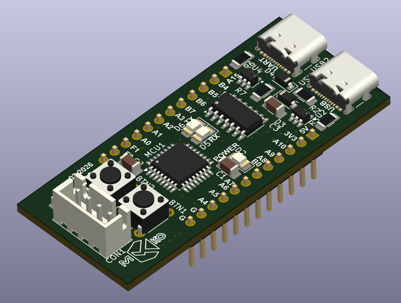
Building a Compact Dual-USB-C STM32G4 Development Board
Most STM32 dev boards on the market force a compromise: either you get a proper on-board debugger and UART bridge with a bulky footprint, or a minimal breakout board that leaves you soldering wires just to get a serial console working. This project splits the difference.
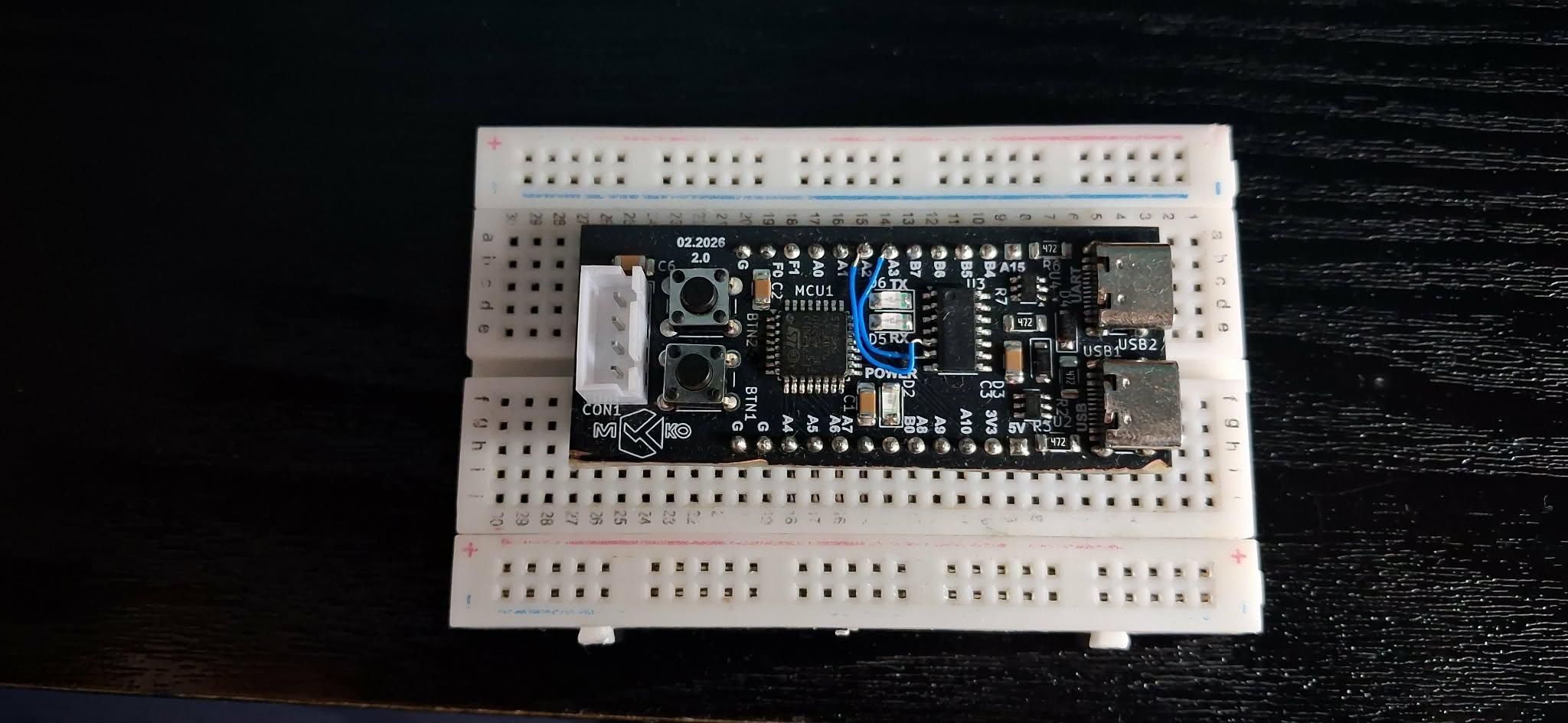
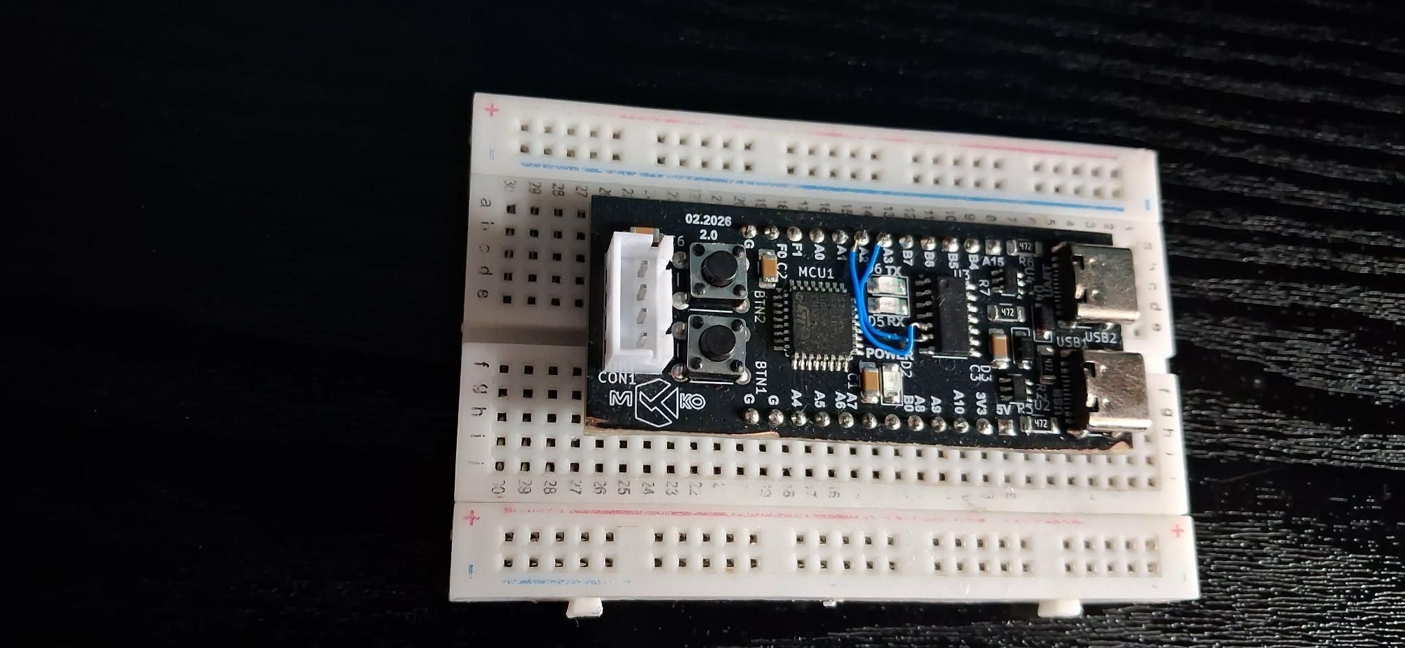
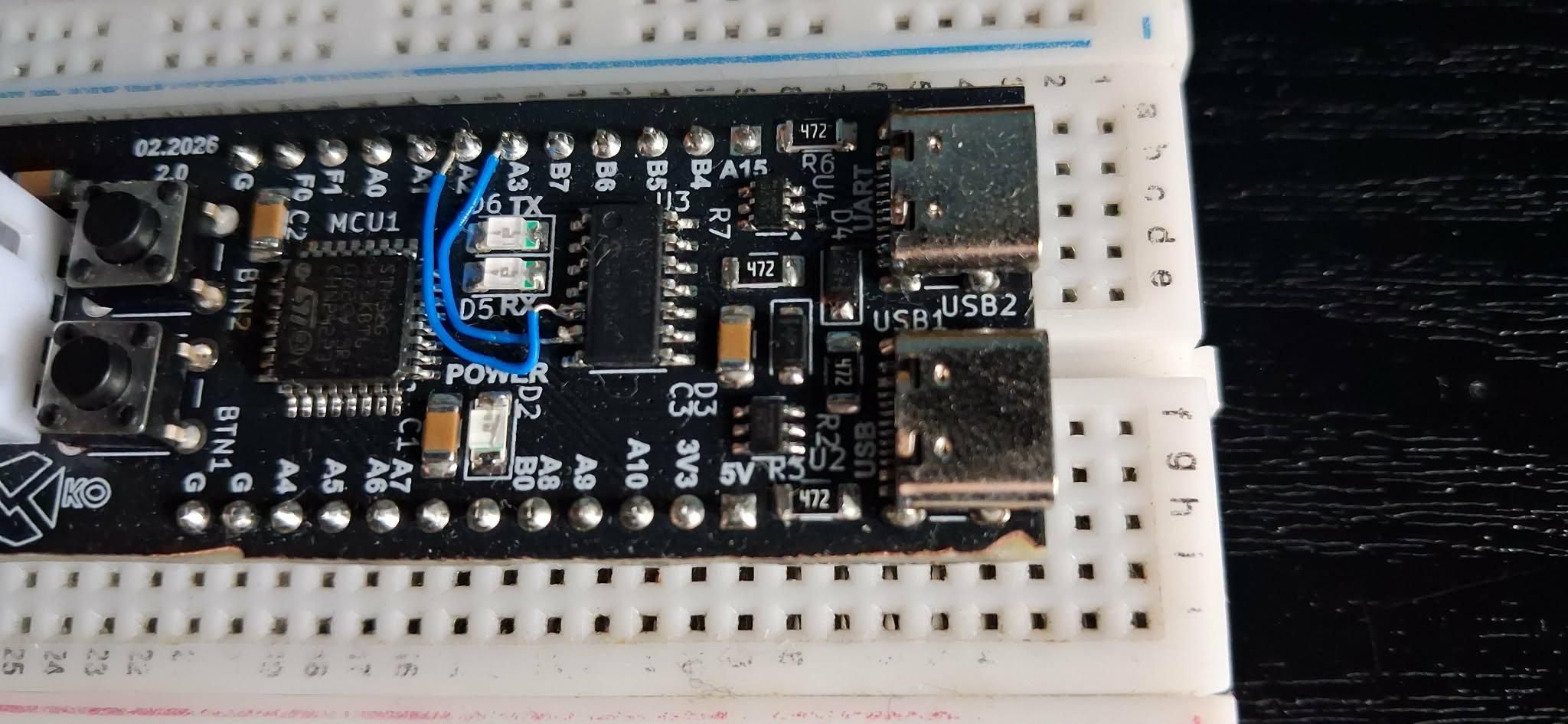
At its core sits an STM32G431KBT6 — a Cortex-M4 running at 170 MHz with hardware math accelerators built in — flanked by two USB-C connectors doing two very different jobs. One routes through a dedicated USB-to-UART/I2C bridge for serial communication and firmware flashing. The other connects straight to the microcontroller's native USB peripheral for full-speed USB device applications. Add a 4-pin SWD header for real debugging, a reset button, and a full set of breakout pins along both edges, and you get a board small enough to drop into an enclosure but flexible enough for serious embedded work.
In this Instructable, I'll walk through the design decisions behind this board: why the STM32G4 instead of the usual F1/F4 suspects, why two USB-C ports instead of one, how the power and debug interfaces are built, and what changed between the previous revision and this one.
Why Build Another STM32 Dev Board?
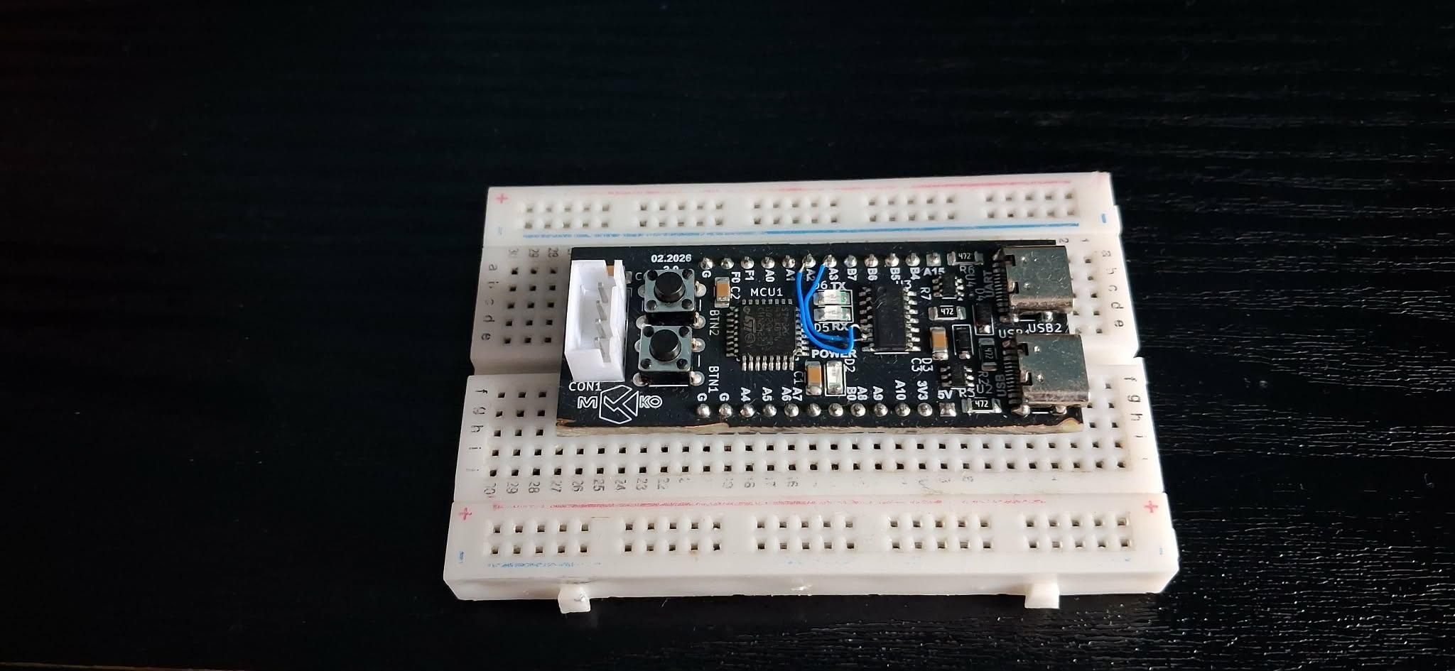
The "pill board" and Nucleo ecosystems already give hobbyists plenty of options, so it's worth being upfront about where this board fits and where it doesn't.
Nucleo boards (ST official):
- Strength: onboard ST-Link debugger, huge community support, works out of the box.
- Weakness: large form factor, often more expensive, and the MCU selection doesn't always include the newer mixed-signal G4 parts in a hobbyist-friendly package.
Black Pill (STM32F411) and similar clones:
- Strength: cheap, compact, native USB for DFU flashing, enormous community documentation.
- Weakness: no dedicated UART bridge (you need a separate USB-serial adapter for a console), and the F411 is a general-purpose M4 core without motor-control-oriented peripherals.
Arduino Uno/Nano:
- Strength: unbeatable beginner ecosystem and library support.
- Weakness: 8-bit AVR core (or a very basic M0 in some newer variants) with no floating-point hardware, no CORDIC, no fast ADC — a real ceiling once a hobbyist wants to move beyond blinking LEDs into signal processing or motor control.
This board's answer to that gap is simple: keep the compact, breadboard-friendly form factor hobbyists like about the Black Pill, but put a more modern, mixed-signal MCU on it, and fold in both debug conveniences (UART bridge and SWD) that usually force a choice.
The honest trade-off: the STM32G4 series has a smaller flash/RAM budget than an F4 (128 KB flash / 32 KB RAM on the G431 vs. 512 KB / 128 KB on the F411) and a noticeably smaller pool of ready-made hobbyist tutorials, since F1/F4 have been the de facto standard for years. Anyone coming from Arduino or Black Pill tutorials will do more of their own HAL/LL reading. That's the price of getting access to newer peripherals.
The Brain: STM32G431KBT6
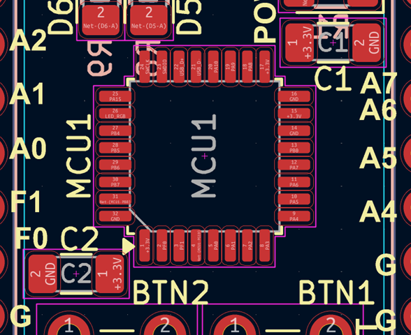
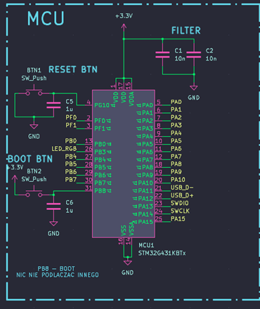
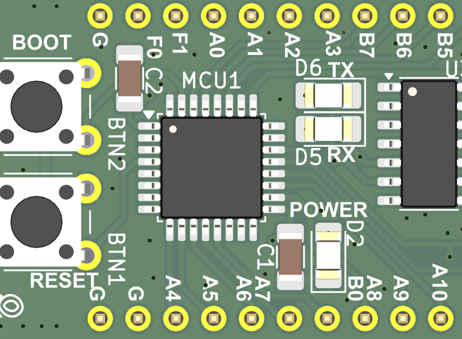
The STM32G431 is part of ST's G4 "mixed-signal" family, and the specific peripherals it brings are the real reason to pick it over an F1 or F4 for anything beyond generic GPIO-pushing:
- CORDIC coprocessor — hardware-accelerated trigonometric and vector operations, useful for motor control (Park/Clarke transforms), DSP, and any application computing sin/cos/atan2 repeatedly without burning CPU cycles on software approximations.
- FMAC (filter math accelerator) — a hardware single-tap FIR/IIR filter block, handy for signal conditioning without loading the CPU.
- Multiple fast 12-bit ADCs running up to several Msps, plus built-in comparators and op-amps — this alone removes several external analog front-end chips that a Blue Pill or Black Pill design would need for the same task.
- 170 MHz core clock with a reasonably efficient pipeline, giving solid headroom over the F411's 100 MHz for real-time control loops.
Where it falls short compared to an F4: less flash and RAM, a USB peripheral that (depending on the exact part number/package) may run in full-speed-only mode without a separate high-speed PHY, and a newer HAL library with less battle-tested example code floating around online. For a "learn embedded systems" board this is a minor inconvenience; for someone trying to port a large existing F4 codebase, it's a real consideration.
Bottom line: if the project's stated goal is a board aimed at motor control, power electronics, or signal-processing hobby projects, the G431 is a genuinely better-suited choice than the F103/F411 chips most clone boards use. If the goal were pure general-purpose learning with maximum tutorial availability, F4 would still win on ecosystem size alone.
Power Architecture: USB-C In, 3.3V Out
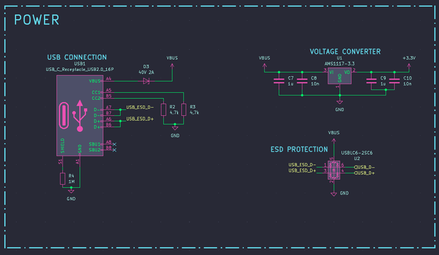
Power arrives at 5V from whichever USB-C port is plugged in, then gets dropped to 3.3V logic level by an AMS1117-3.3 linear regulator (LDO).
Why an LDO makes sense here:
- Extremely simple: three pins and two capacitors, no inductor, no switching noise. That matters on a board carrying fast ADCs — switching-regulator ripple is exactly the kind of noise that leaks into analog measurements and degrades ADC accuracy.
- Fast transient response suits a dev board with unpredictable current draw (button presses, peripherals toggling on and off).
- The AMS1117's 1A rating is far more than the MCU and bridge chip need in practice — combined draw is well under 200 mA under normal use.
Where the LDO approach costs you:
- All the dropped voltage (5V → 3.3V, roughly 1.7V across the load current) is wasted as heat rather than delivered as useful power. Efficiency tops out around 65–70%. Fine at low current; it becomes the limiting factor fast if a user wants to power external 3.3V sensors or displays directly off this board's rail.
- AMS1117 counterfeit parts are a well-known problem in the hobbyist PCB world. A large share of AMS1117 chips sold through generic/untraceable channels don't actually meet the datasheet's line and load regulation specs. Boards can work perfectly on the bench with one reel and then show a marginal, noisy 3.3V rail with a different batch from a different supplier. This is worth flagging explicitly to readers who are sourcing their own parts rather than following an assumption that "AMS1117 is AMS1117."
- Dropout voltage (~1.1–1.3V near full load) isn't an issue here given the 1.7V of headroom from 5V, but it does mean this exact regulator choice would not work if the board were ever adapted to run from a single-cell LiPo (~4.2V down to ~3.0V) instead of USB.
A better alternative worth considering for a future revision: the AP2112K-3.3 (Diodes Inc., SOT-23-5) is essentially a drop-in-class alternative — smaller footprint, tighter output accuracy, and built-in current limiting and thermal shutdown, at a similar unit cost, and it's far less commonly counterfeited than the AMS1117. For a logic-only rail like this one that only ever feeds the MCU and bridge chip, I'd call this the more "modern" choice. This isn't a criticism of the current design — AMS1117 from a reputable supplier works fine at these current levels — just a note for anyone doing a v2.2.
Debug & Programming Interface: the MCP2221A USB-UART Bridge
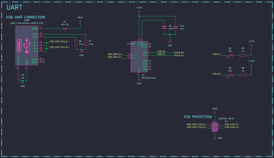
This is one of the more distinctive component choices on the board. Instead of the usual CH340, CP2102, or FTDI FT231X, this design uses Microchip's MCP2221A — a USB-to-UART and USB-to-I2C bridge that also exposes four GPIO pins (some with ADC/DAC capability) and enumerates on the host as a composite USB device.
Comparing the common options:
- CH340 — cheapest, but driver installation is often required and can be flaky on newer macOS versions; also one of the most commonly counterfeited USB-serial chips on the market.
- CP2102 — solid driver support, but usually still needs a separate driver install on Windows.
- FTDI FT231X — excellent throughput (up to ~3 Mbps) and driver maturity, but FTDI is historically the most targeted chip for counterfeiting, to the point that FTDI's own drivers have in the past deliberately bricked non-genuine parts.
- MCP2221A — enumerates as a CDC (Communications Device Class) device, meaning it uses inbox drivers already present in Windows 10+, Linux, and macOS. No install step at all for the end user.
Why this fits a hobbyist dev board well:
- Zero-driver-install "plug in and it works" experience, which matters a lot for a board aimed at people who might not be comfortable troubleshooting a driver conflict.
- The onboard I2C master and GPIO/ADC/DAC lines are effectively a free bonus: the same USB-C port could, in principle, double as a standalone USB-to-I2C debug adapter for probing other boards, independent of the STM32 entirely.
- Microchip's supply chain has historically had less of a grey-market clone problem than CH340 or FTDI parts, reducing the "why doesn't my $2 adapter work" failure mode.
Trade-offs to be upfront about:
- Practical UART throughput is more modest than FTDI or even CH340 — comfortable for printf-style debug logging and bootloader flashing, but if a project needs to stream high-rate sensor data over serial, this chip (not the STM32) becomes the bottleneck.
- It's a less "famous" chip than CH340 or FTDI, so very old Linux kernels might lack the relevant CDC-ACM module by default — vanishingly rare with any modern distro.
- Slightly pricier than a bare CH340, which matters if cost-competing with sub-$5 clone boards is a goal.
Verdict: for a board explicitly designed to be beginner-friendly and modern, the MCP2221A is arguably the better choice over CH340 — trading some raw baud rate for a zero-hassle driver story and free bonus I2C/GPIO capability that costs nothing extra in board space, since the chip needs to be there anyway.
SWD Debug Header
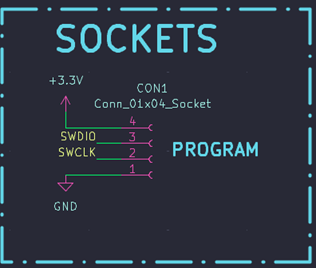
Alongside the UART bootloader path, the board includes a proper SWD connector: 4 pins on standard 2.54 mm pitch, carrying SWDIO, SWCLK, GND, and NRST.
One naming note: a plain 2.54 mm pin header is technically not a "JST" connector. JST is a manufacturer whose branded series (PH, XH, SH, etc.) use smaller pitches — typically 2.0 mm or 2.5 mm — with a positive locking latch. What's on this board is a standard 0.1" pin header, most likely unshrouded. Worth stating precisely in the article since it determines what cable a reader needs to source.
Why having SWD at all matters: the STM32's built-in USART bootloader (used over the MCP2221A UART bridge) can flash firmware, but it gives no breakpoints, no live variable inspection, and no fault register access. SWD is what lets a user step through code and actually diagnose a hard fault instead of guessing. Including a proper debug port here, rather than relying on the bootloader alone, is the same choice serious dev boards (Nucleo, Discovery) make and most bare clone boards skip.
Including NRST specifically matters too: without a hardware reset line, recovering from a firmware hang that disables the debug port (an errant low-power mode, a misconfigured clock tree) can require strapping boot pins or a full mass-erase via the bootloader instead of a clean debugger-triggered reset. Small detail, meaningful difference during actual debugging sessions.
What's missing compared to a full ARM debug connector, and why it's an acceptable trade here:
- No VTref/VCC sense pin. A standard 10-pin Cortex Debug header includes this so a probe can auto-detect the target's logic level and configure its I/O drivers accordingly. It's omitted here — which works fine because the board is hard-wired to 3.3V, so there's no ambiguity to resolve — but it does mean this connector won't plug into a "universal" debug cable without the probe being told to assume 3.3V, or a manually wired adapter.
- No SWO (trace) pin. Fine for flashing and breakpoint-level debugging; rules out real-time ITM/SWO trace logging, which matters more for timing-critical control-loop work than general firmware bring-up.
- Unshrouded 4-pin header risk. Without a key or shroud, a cable can physically be seated reversed or offset by one pin, which on this pinout could short SWDIO to GND or backfeed NRST. Not usually damaging, but a clear pin-1 silkscreen marker is important — worth confirming that's visible in the photos.
Suggestion for a future revision: either move to a shrouded/keyed header (cheap insurance against reversed cables) or, space permitting, expand to 5 pins to add VTref — that single addition would make the board compatible with off-the-shelf ARM debug cables instead of requiring a custom-wired one.
Native USB: the Second Port
The second USB-C connector bypasses the bridge chip entirely and wires straight to the STM32's own USB peripheral pins. This is what lets the finished project actually be a USB device — CDC serial, HID, mass storage, or a custom class — independent of the programming/debug path.
Why split this from the UART bridge port instead of sharing one connector (the way a Black Pill shares a single micro-USB between native USB/DFU and everything else): on a single-port board, a UART debug console and a live USB application can't be connected at the same time — the user is constantly unplugging and replugging to switch contexts. With two separate ports, firmware can be flashed and debugged over serial through one cable while a USB host application is being tested live through the other. For anything implementing a USB device class, that parallel workflow is close to mandatory during development, not a nice-to-have.
The honest cost: a second USB-C connector, a second set of ESD protection components, and extra board area — plus, for an absolute beginner, one more "which port do I plug in" decision that a single-port board avoids. Clear, separate silkscreen labeling for the UART and USB ports (already present on this board) is what keeps that from becoming a real point of confusion.
Version History: What Changed From V1 to V2.1
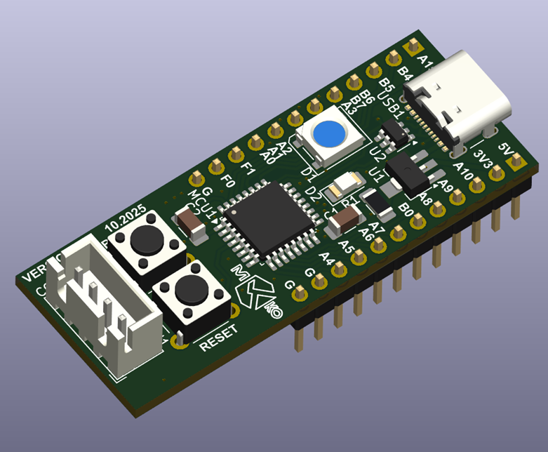
The previous revision of this board had neither the onboard UART bridge nor the second, dedicated USB-C port — using it meant keeping a separate USB-to-serial adapter on hand any time a serial console or bootloader flash was needed.
Folding both of those into the board itself is the same evolutionary step official Nucleo boards took over bare "pill" boards years ago: trade a bit of extra BOM cost and board area for a genuinely self-contained, single-cable development experience. It's a meaningful usability jump — no more "where did I put that FTDI adapter" before starting a session — and it's the main functional difference between this revision and the one before it.
Design Tools
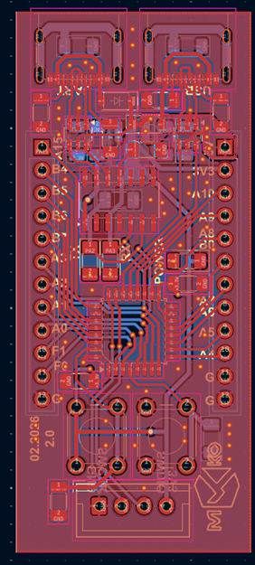
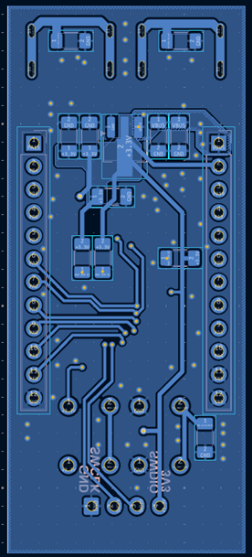
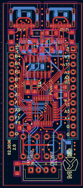
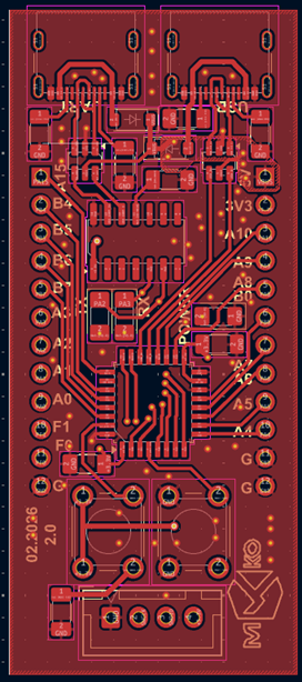
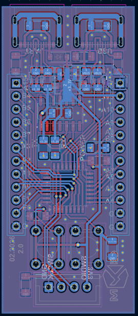
The board was designed entirely in KiCad. Gerbers and full project files aren't being published alongside this article, but the schematic-level decisions covered above — MCU selection, dual USB-C topology, LDO regulation, MCP2221A bridge, and SWD header layout — should be enough for anyone wanting to design something similar from scratch or adapt the concept to their own MCU of choice.
Downloads
Final Thoughts
This board isn't trying to out-cheap a Black Pill or out-support a Nucleo — it's aimed squarely at hobbyists and embedded enthusiasts who've outgrown Arduino's 8-bit ceiling and want access to a modern mixed-signal MCU (CORDIC, FMAC, fast ADCs) without giving up the compact form factor and single-cable convenience they're used to.
The trade-offs are honest ones: less flash/RAM and a smaller tutorial ecosystem than F1/F4-based boards, an LDO that caps how much external hardware can be powered off the 3V3 rail, and a debug header that assumes a fixed 3.3V target rather than supporting universal debug cables. None of these are design flaws so much as reasonable choices for a board with this specific goal — and each one has a clear, low-cost path to improvement in a future revision (AP2112K regulator, keyed SWD header with VTref) if that goal shifts.
For now, it does exactly what it set out to do: one small board, one modern MCU, two USB-C ports doing two different jobs, and a real debug port — no separate adapters required.