Milling Printed Circuit Boards (PCBs) on a Cheap CNC Machine
by mattwach in Circuits > Electronics
41980 Views, 251 Favorites, 0 Comments
Milling Printed Circuit Boards (PCBs) on a Cheap CNC Machine

 on a Cheap CNC Machine)


This guide presents an entire end-to-end process of milling PCBs with a "cheap" 3018 CNC machine (although other CNC machine types can also be used).
Part of that process, verifying the design and calibrating the machine, are helped along with simple Python scripts that I created and am sharing as free open source. This guide explains how to to use these optional tools in the appropriate places in the process.
Even if you do not use the tools, I think there's helpful information here - both for beginners and more experienced individuals looking to compare notes.
Time Estimate
This document ended up being a bit long. Does that mean that the process takes a long time? I don't think it does. Here are some time estimates:
- As a beginner, I would estimate around 6 hours to do a small project from start to finish (starting with drawing up the schematic). Much of that time will be spent learning how to use the software tools.
- After gaining some experience, I would expect around 2 hours of work for the same result assuming you are working at a moderate pace.
Resources
All of the project files I mention in this document can be found in this github project that I created: http://github.com/mattwach/cnc_pcb_tools
Disclaimer
I have tested these tools and process and they work well for me. That said, all tools and advice presented in this document are at your own risk - I take no responsibility for anything that goes wrong!
Supplies
- CNC Machine. I'm using a SainSmart 3018 CNC mill which is on the cheaper end of the spectrum. Here is a even less expensive variant that should work just as well. Really, anything that can do precision movement will work.
- CNC Bits. I like these for starting. I discuss the options in more depth later.
- Copper Clad Boards. Here is one example. You might need a larger size eventually.
- Spoil board. Something to put between the copper clad and metal CNC table for drilling and cutting out. I like the convenience of the linked product but you can also clamp down a piece of scrap wood.
- Wide Painters Tape. Used for securing the PCB to the spoil board.
- CA glue. Also called "superglue" Used with the painters tape.
All of the software used in this guide is free. Each software package also has alternatives which I'll give an example of but do not go into further details.
Why CNC a PCB?

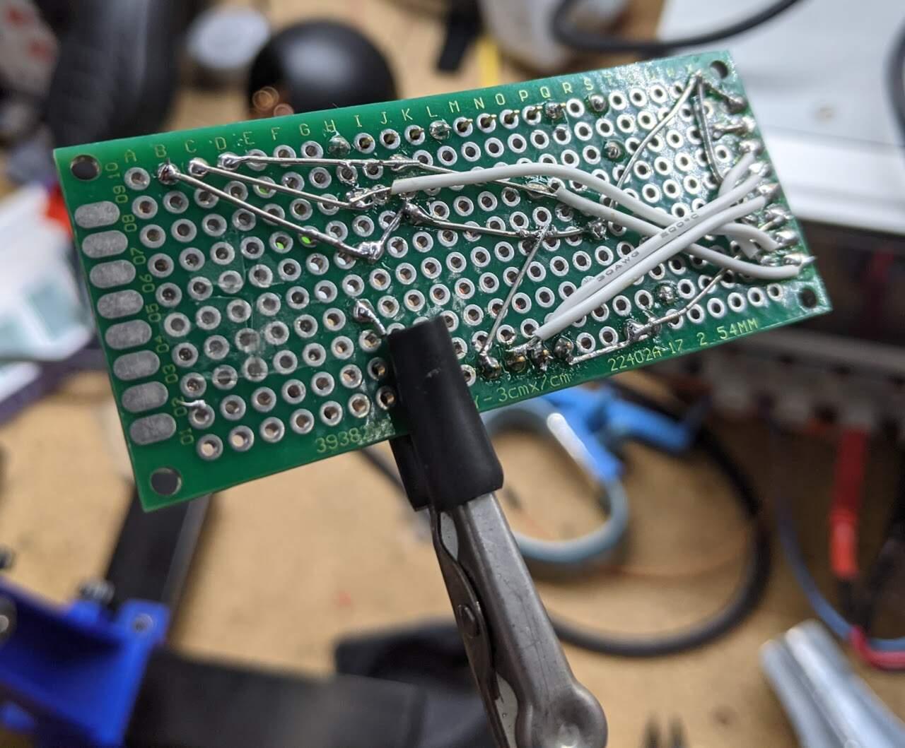


CNC isn't always the best choice for a project but I believe it has its place. I've created many projects with each of the following methods:
- Breadboard
- Prototype Boards
- CNC (this doc)
- Ordering a PCB from a fab, such as oshpark.com or www.pcbway.com
Every option above has it's trade-offs. Below I'll offer a brief opinion on each one:
Breadboard
Breadboards are great for trying out something quickly. Parts are not "consumed" and can be reused. Using prebuilt modules as "blocks" simplifies wiring.
However, any interconnects in your design will be performance limited in terms of frequency, stray capacitance, unintended resistance and connection reliability. It's not all bad since you get to exercise some troubleshooting skills and things seems to work fine most of the time.
Prototype Boards
Like a breadboard but with better reliability and permanence. Making one of these is a bit labor intensive though and there are few economies of scale when making multiple copies. Operating frequency is also usually limited due to the lack of careful layout, stray capacitances and the lack of a ground plane.
CNC
Performance are reliability are excellent. Both SMD and through-hole components are supported.
Single-sided boards are a good fit. Simple double sided boards also work well (often just a few hand-wired patch wires on the back is enough). CNCing both sides of a board (for complex designs) is possible but requires alignment techniques that are out-of-scope for this guide.
Soldering is less convenient than a manufactured PCB due to lack of a solder mask. Lack of a silk screen (labeling) means that you may need a PCB printout to guide component placement.
Chemical Etch
I have not tried this one yet (and am meaning to soon) but have read and watched videos on the process. Overall, it seems similar to CNC - perhaps a bit easier to dial in the process and get good results. There are some clear downsides however. One is having to work with some nasty chemicals that literally dissolve metal. A second drawback is that drilling holes and cutting out the board are not handled by the process.
Ordering a PCB
If you need many copies, > 2 layers, or have a complex design, ordering a manufactured PCB is your best option. You also get a solder mask for easier soldering and a silkscreen to label component and provide other notes.
Turn around latency is around a week. Cost is in the $20-$60 range (including shipping) assuming that your board design is perfect. If not, you'll consume additional weeks and money on iterations (thus many designs, including commercial products, have unpopulated "just in case" areas as a form of insurance).
Design Your Schematic
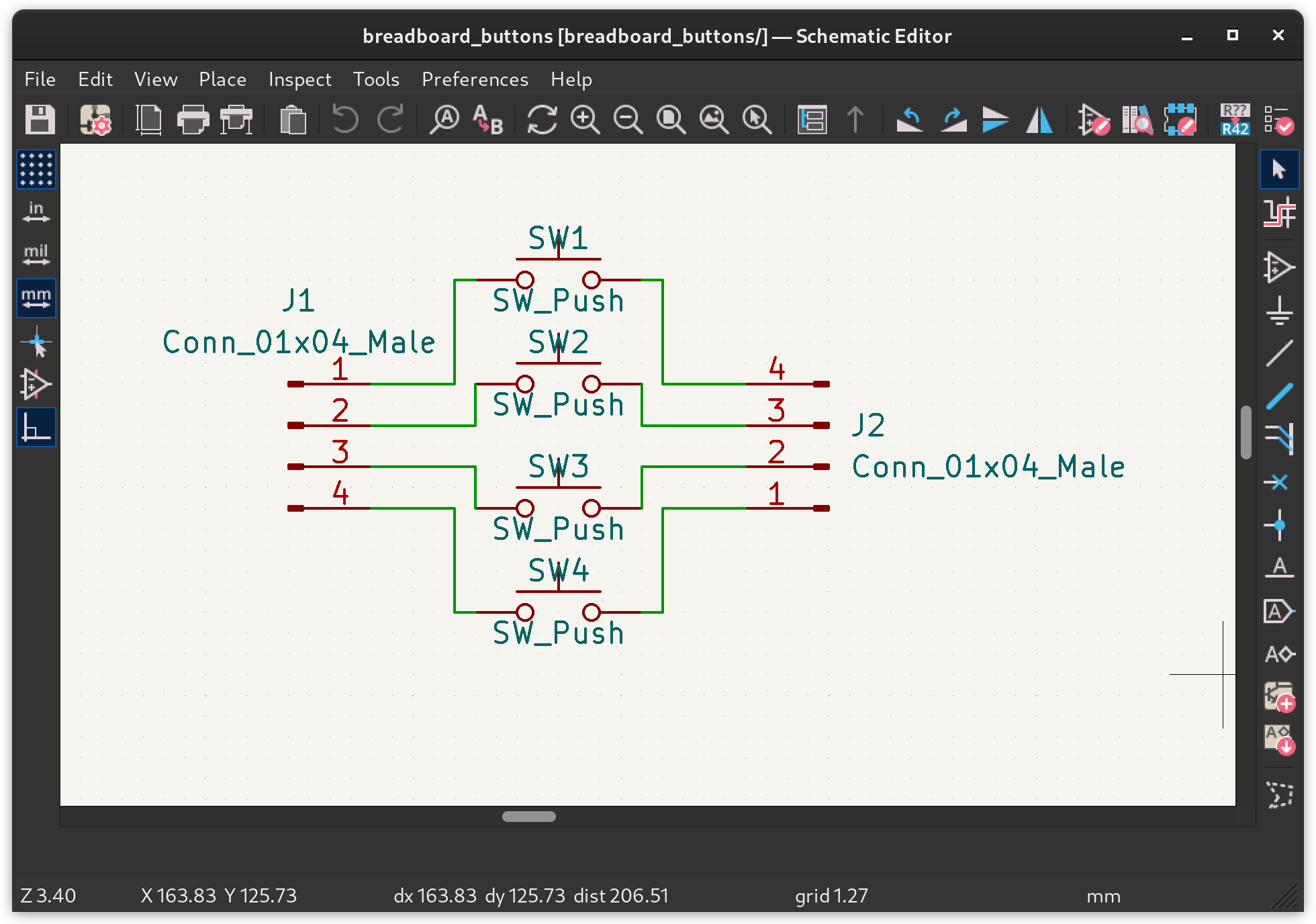


The first step to CNC is creating a schematic in an appropriate software tool. I'm going to use KiCAD. I used to use Eagle but many agree that KiCAD has surpassed it. Eagle and many others will still work fine, however, as they can all export Gerber plots (the "handoff" data format).
Some complex circuits require fine traces and tight spacing to allow for placement of tiny surface-mounted components. These are possible with CNC but do not make an ideal beginner project. While learning, a more forgiving project will help you be successful as you learn. My suggested starter project is thus a simple button adapter for breadboards. See above for the schematic.
This design is good to start with because it is quick to CNC and has forgiving tolerances. It's also useful as standard buttons do often do not fit securely in a breadboard as these will. Finally, it has a mix of surface mount and through-hole components.
Looking at the schematic, there are two pin headers and 4 buttons. For the Pin header PCB footprint, I'm just using a pin header built into the standard library:
If you are just starting with KiCAD, one way to set the footprint is to click on it in the schematic, then type "e" to bring up its dialog, where you can select the footprint. I also suggest watching some of John's Basement KiCAD tutorial (or similar).
Layout Your PCB


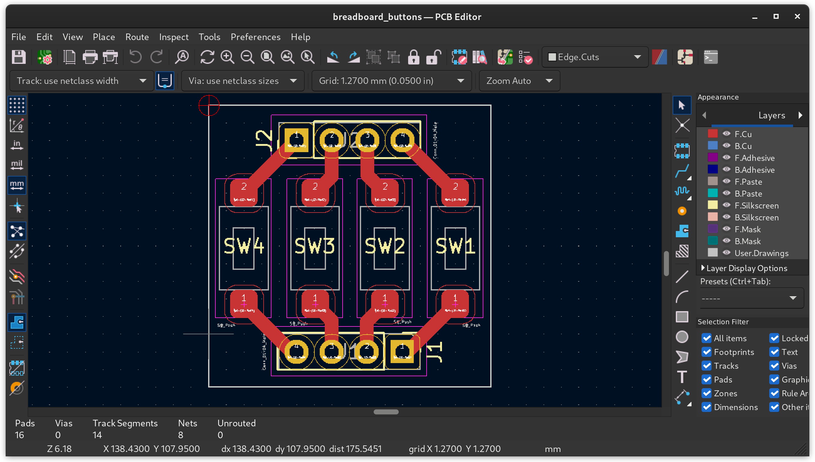

Above is an image of the SMD buttons I chose. They are 6x3.5mm. I could not find any footprints for these in the KiCAD library. The files probably exist somewhere on the internet, but it's really quite fast and easy to make a custom one in KiCAD (using the Footprint Editor), and that is what I did. John's Basement, video #12 demonstrates how to do this.
Of course, you can just use the one I already placed in the examples/ folder if you are going with the same button and want to focus more on the CNC steps.
The third image above shows the completed/routed PCB.
Beginner Note: This circuit doesn't have a ground connection, which is a bit unusual. For a design with a ground, you'll want to Google search how to do a "ground fill" in KiCAD as it can simplify wiring and help reduce electrical noise in your circuit.
Design Constraints
If you choose File -> Board Setup... in the PCB editor, you'll should see a dialog of settings, one of which is Design Rules: Constraints. Here, there is a "minimum clearance" and "minimum track width" setting that you can use to make your CNC life easier (in trade for limiting the ability to route tiny parts). I think 0.4mm for both settings is a good setting because:
- You can use more robust bits that cut a bit wider.
- If your cuts are not perfect, the board will likely still be usable.
of course, the setting are just for less-complex designs that can support it. Once you have a dialed-in process, you can push these numbers as small as you want to try for.
Plot Gerber Output Files


Regardless of what software tools used to design the PCB, the design needs to be exported in a universal format that the next phase of the process can understand. These files are known as "Gerber" files and are like a "PDF" or "STL" for circuits. Gerber files capture only the shapes of the PCB layout and not other information, such as the associated schematic.
In KiCAD, you create Gerber files using File -> Plot. The first image above shows a dialog with the settings I use.
Note that I'm only exporting the F.CU and Edge.Cuts layers. If you were sending these files to a fab, they would want other layers, like the silkscreen layer.
This particular design needs holes drilled for the pin headers and that data needs to be exported too. "Generate Drill Files..." in the plotting dialog will bring up a drill-specific dialog. The outputs are "PTH" and "NPTH" files. Those stand for "plated hole" and "non plated hole". This design only has plated holes but, if you have mounting holes, then both files might have some data in them.
Gerber to GCode Using Flatcam

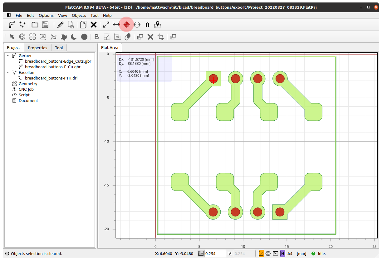
There are a number of tools that can convert your exported Gerber files (from the previous step) into GCode files that your CNC machine can use. One that I like is Cambam, which is a great all-around CNC program. But Cambam is not a free program so we are going to go with Flatcam, which is free. Flatcam is a bit more complex than it needs to be and is not bug-free but it gets the job done once you find a navigation path through it's large set of options. Let's jump in:
- Install and start the flatcam software.
- Load up all of the Gerber files (first and second image)
- Load the drill files (3th and 4th image)
- Note the horizontal and vertical red lines. These will be the [0, 0] origin of the CNC machine. It can be set in KiCAD or Flatcam using the crosshair tool. I like the upper-left corner of the design because it makes it easy to avoid my depth probe (more on that later).
Go ahead and save the project.
Generate Copper Geometry

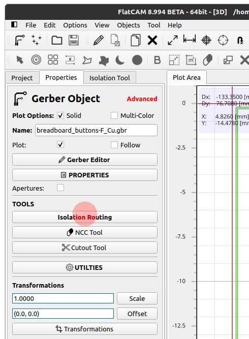


Our CNC machine needs a GCode file to cut copper traces. Flatcam has us get there in two steps: First we convert Gerber to a geometry object, then we convert this geometry object into GCode. Let's do the first part now:
- Select the copper layer, then "properties" (first image).
- The properties dialog is a launchpad for doing a number of things. For the copper layer, we want to choose "Isolation routing" (2nd image).
- Now we presented with settings for the isolation tool (3rd image)
CNC Bit Setup (3rd image, Red Mark #1)
- Here we choose the bit type and properties. These settings are complexity overkill, in my opinion. The intent is that the tool wants to help you calculate the needed depth for V bits to get the isolation width you want. The reality is that the calculations assume your machine and process have perfect tolerances (e.g. no bit runout, perfect cuts, perfect positioning). If any of these are untrue, and the probably are, then you just end up putting in adjusted numbers anyway to get the final result to come out.
- To keep things simple, I directly choose the final cut width. I do this by choosing a "C1" bit type, then directly type in the expected cut width of 0.39mm. I'm essentially telling flatcam "trust me, the cuts will be 0.39mm wide". If the real cuts are a little wider or narrower, it's usually not a problem.
- I chose 0.39mm because I chose 0.4mm isolation widths in KiCAD earlier. Whatever "isolation width" design constraint was chosen in your PCB layout tool needs to exceed the number you enter here. Otherwise flatcam will silently omit traces where it can't fit a line.
Passes and Overlap (3rd image, Red Mark #2)
- Passes are the number of cut lines to make around each trace.
- Overlap is how much to overlap the passes. Too little overlap will lead to small bit of copper remaining between each pass, which usually isn't a big deal.
- "Follow" and "Isolation Type" can be kept at default settings.
Generate Geometry (3rd image, Red Mark #3)
- Create the geometry traces for out next step. You can actually click this button multiple times (presumably with different settings) to create multiple geometries - then ignore, hide or delete the ones you are not planning to use.
The 4th image shows results with 3 passes and 25% overlap. Now is a good time to save
Generate Copper GCode
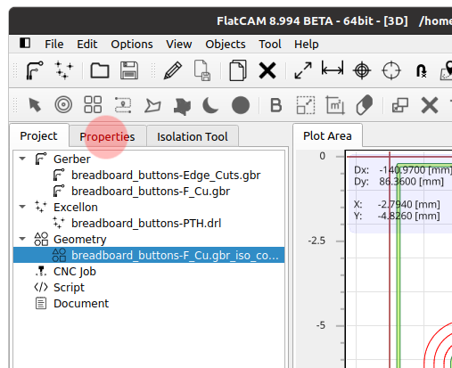


Now we convert the geometry object to the final gcode file. To do this flatcam needs more information. Click on the geometry object, then properties (first image). The second image shows the dialog that opens up. Going through the dialog:
Red Mark #1
This section helps you calculate your cut depth if you are using a V bit. As I said earlier, I find it easier to choose the "C1" bit type and put in the depth myself. Thus if you are following my path, you can simply ignore this section.
Red Mark #2
- Cut Z: How deep to cut. A very important parameter. With a V bit, it also will determine your cut width (deeper cuts wider due to the V shape). Cut depth also has a big effect on how likely you are to break a bit. I usually go with -0.05mm.
- Multidepth. This setting allows you to split your cut into multiple passes. There are ways to do this "dynamically" later in the process thus I don't use this option for copper isolation.
- Travel Z: How high to hover the bit over the board when not cutting. The default is fine for starting out.
- Feedrate X-Y: How fast to cut in the XY direction. I use settings in the 120 to 200 range and found through controlled experiments that the quality was similar. There is surely too high of a setting where quality and bit health will suffer and of course that limit will depend on your hardware.
- Feedrate Z: How fast to plunge. I find the default setting of 60 to be ok and have not experimented further.
- Spindle Speed: RPM of the motor. With a stock 3018, this number is not accurate because these machines have no RPM sensor. 10000 basically means "full power" which will be ~7500 RPM in with a typical 3018 stock motor.
Red Mark #3
- End Move X,Y,Z: Where you want the bit to end up when the job is done. I find ending at a x,y of 0,0 is nice when changing bits.
- Preprocessor: Used to tailor the GCode output to a type of machine. If you have a 3018 machine, you probably want a GRBL variant. You can also make your own preprocessor template from an existing one - something to consider after you get more experience with the process.
Red Mark #4
Click "Generate CNC object" Now you have a "simulated" CNC plot and an option to save it (third image).
Here is a quick look at what was saved:
  (G-CODE GENERATED BY FLATCAM v8.994 - www.flatcam.org - Version Date: 2020/11/7)

  (Name: breadboard_buttons-F_Cu.gbr_iso_combined_cnc)
  (Type: G-code from Geometry)
  (Units: MM)

  (Created on Saturday, 27 August 2022 at 10:30)

  (This preprocessor is used with a motion controller loaded with GRBL firmware.)
  (It is configured to be compatible with almost any version of GRBL firmware.)

  (... MORE COMMENTS REMOVED ...)

  G21
  G90
  G17
  G94

  G01 F120.00

  M5
  G00 Z15.0000
  G00 X0.0000 Y0.0000
  ( --- LOOK HERE --- )
  T1
  (MSG, Change to Tool Dia = 0.3900)
  M0
  G00 Z15.0000

  M03 S10000.0
  G01 F120.00
  G00 X2.0236 Y-7.7442
  G01 F60.00
  G01 Z-0.0500
  G01 F120.00
  G01 X2.0370 Y-7.7495 F120.00
  G01 X2.0923 Y-7.7691 F120.00
  G01 X2.1584 Y-7.7856 F120.00
  G01 X2.2259 Y-7.7957 F120.00
  (... MORE COMMANDS ...)
Check out the LOOK HERE section above. My particular machine does not like the T1 (tool change) code, your's may be OK with it. A CNC dry run, explained later, will allow you to safely validate the file and make the needed tweaks.
Another thing to look for is the M03 S10000.0 line. This line tells your motor to spin up (at 10,000 RPM). If you forgot to set your RPM (left it at zero), this line will be missing and you will be sad when the not-spinning bit breaks on the copper plate.
Sanity checking Z cut depth is also advised. Above the G01 Z-0.0500 tells us it will be -0.05mm, which was the intent.
Wouldn't it be nice if the computer did all of this checking for you? The tools I have provided in my github project do exactly that (e.g.: check_pcb_cu.py <filename>). Computers are way better than me at checking so I just run the check tool every time to help find errors before running the machine.
Generate Drill GCode

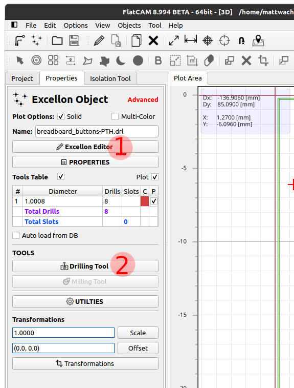


First I disable (not delete) the isolation geometry and CNC plots to clean up the plot a bit (first image).
The second image shows the settings dialog for drills. Looking at each highlighted step:
- The "Excellon Editor". For this project we have 8 holes to drill and they are all the same size so we don't need this option. But, this option is often useful as it is often the case where you have several drill sizes (like 0.85, 0.9, 0.95) and you want to combine them all into a single size (all 0.9 for example) to simplify the job.
- Is the drilling tool. Clicking on it brings up the third image.
Looking at the drilling options (third image)
- The drills you want to include in this file. We only have one type in this example, so nothing further to do here.
- How deep and fast you want to drill.
- Cut Z: should be the same as your board thickness, maybe plus 0.1mm or so.
- Multidepth: Should not be needed for drilling
- Travel Z: hover height. default is fine.
- Feedrate Z: cut speed. Depends on the bit you use and the diameter of the hole. For small holes, the 300 setting is fine.
- Spindle Speed: As-described in the previous (copper) section
- Offset Z: It's just added to Cut Z for tapered bit. Or you could have just changed Cut Z directly so I'm not sure why this exists.
- As-described in the copper section (common parameters)
- Click here to make your drills
Now the drill paths are made and it's time to save the gcode file (4th image).
Generate Edge Cut GCode


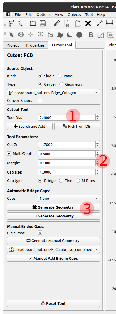


Edge cuts are the cuts around the edges of your board.
- First choose the edge cuts gerber file and choose "Properties" (first image).
- Choose the "Cutout Tool" (second image)
Now we see the cutout properties (third image). Each highlighted setting is described below:
- Set this to the diameter of your cutout bit. I go with something in the 2-3mm range here.
- The defaults as-shown work fine for me. Set Cut-Z to the thickness of your board plus 0.1mm. Here we do want "multidepth" selected so that the bit takes several passes to do the cut as trying to cut everything in one pass would put a lot of load on the cutting bit.
- I have "Bridge Gaps" set to none. If you set it to something else (like 4), then the CNC machine will leave small tabs that connect the board to the copper clad. I use the "double sided tape" method (described in the CNC section) so I do not need any tabs.
When you are all set, click on "Generate Geometry" (top one). This brings up the dialog in the 4th image:
- Verify this is the diameter of your cutting bit
- The parameters are similar to the copper section except that we are going with multidepth for this cut. Make sure spindle RPM is not zero.
- The common section is the same as the copper section. Make sure that the preprocessor is set as-described in the copper section. Note that changing the preprocessor can reset other settings so check them over after making a change to this option.
- Generate the tool paths
All that is left to do is export the gcode (5th image)
And we are done! It may have seemed like a lot of work but it goes pretty quick (a few minutes) after you've done it a few times.
I suggest saving your project at this point.
CNC Machine Setup




Machine Properties
The machine I'm working with is a 3018 Sainsmart. I've also done this process on a friend's differently-branded 3018 machine with success. Many machines can be made to work here but clearly some process adaptation will be needed.
Bit Choices
I did extensive controlled testing on many different types and sizes of bits to determine which ones I would use. Below are the "winners" of this testing.
Isolation routing (Making Copper Traces)
- The first option is the 20 degree V bits that are bundled with many CNC machines. These bits can produce some fine traces and nice detail. They are also quite cheap. On the downside, they are not the designed for cutting PCBs and the associated cutting stress exposes inconsistencies in quality. I found that success with these bits is a combination of cutting very slowly, not cutting too deeply and getting a little lucky.
- Many go for 30 degree V bits as an alternative (2nd image). These bits are a little more robust than the 20 degree bits. The trade-off is that cutting deeper results in a wider track so you will not be able to get as narrow of a track width as 20 degree if it matters (and for many projects it does not).
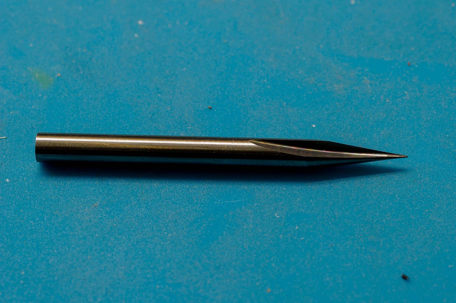
- Next up are 20 degree V bits with an actual cutting flutes (3rd image). I find these to be much more robust than the previously-mentioned bits. They are forgiving to a wider range of cutting speeds and depths. The downside is the minimum track width - around 0.4mm. This may be a non-problem or a deal-breaker depending on your project.
- I final one I'll mention is a bit that is designed for isolation routing (4th image). I find this bit gives the best overall results. But they are (currently) $15 per bit. These are a bit more fragile than the 20 degree fluted bits and you need to watch your cut depth more closely (because they are 45 degree bits) both in terms of cut width and avoiding a breakage. I feel this bit is one to "graduate to" after you are confident in your process.
Hole drilling
For hole drilling, you can use special purpose drill bits (5th image) or repurpose an end-mill bit for drilling (6th image). A specialized drill bit makes cleaner cuts but I find the end-mill to be "good enough" for those cases where you don't have a correctly-sized drill bit handy.
Board cutout
Here I find a standard end-mill bit in the 2-3mm range works well (final image).
Optional: CNC Dry Run Verification

I highly recommend doing a dry run before doing your first real cuts. After you get a couple successful projects behind you, you can skip the dry run.
To do this, first connect the Candle (or equivalent) software to your machine and start it. Next follow these steps.
- Remove any bit that is in the (real) machine
- Use the jogging controls to place the motor head in a safe region. If you are cutting something small (as recommended), the middle of the machine and maybe 3 cm (or so) away from the board is a good spot.
- Click Zero XY
- Click Zero Z
- Load one of your gcode files into candle (like the edge cut file, for example)
- Click the "check mode" option.
- Click "send". This sends each gcode to the machine in a testing mode where the machine will give errors if it gets a code it doesn't like but will do nothing if the code is OK.
- If all is good, unclick "check mode" and click "send" again. Now the machine will start spinning up and moving - it thinks it's cutting but there is no bit loaded and plenty of clearance so you can just watch it for reasonable-looking behavior. Be ready to click "Abort" if anything looks like it is going wrong.
If the machine appears to be doing the right thing, repeat steps 5-8 for each remaining gcode files (copper isolation, drills, test file)
You might see an unrecognized gcode error in step 7. Often these are "tool change" codes (M6, T1) that you can delete from the gcode file with a text editor with no ill effects. If in doubt, look up the gcode on Google. For future projects, you can change the "Preprocessor" in Flatcam (or make a custom one) that permanently omits these codes.
Optional: GCode Validation
Sometimes when driving the creation tools (in this case KiCAD and Flatcam), I accidentally enter an incorrect value in one of the parameter dialogs. The example I'll share is that I once entered -0.45mm for a z-cut depth into the copper - what I meant to enter was -0.045mm. The result what that I broke a $15 bit and two more $2 bits before finding the problem.
The solution I came up with is "validation" scripts. These are simple Python scripts that you feed your final GCode into. They read in the GCode and look for problems.
The problem I mentioned in the previous paragraph will be caught by the checking program along with many others. Which problems exactly? My scripts currently look for:
- Cutting fast, too deep, or out of bounds
- Not spinning up the motor
- Forgetting to choose multipass on edge cuts
- GCodes that your machine does not recognize (e.g. choosing the wrong preprocessor in flatcam)
The script are intended to be easily modifiable for your own needs - you can tailor the rules to be as rigid or flexible as you want.
Here is the actual output of running the three gcode files I generated earlier in Flatcam.
First the copper check (check_pcb_cu.py):
  python3 check_pcb_cu.py breadboard_buttons-F_Cu.gbr_iso_combined_cnc.nc

  Properties:
   lines: 5063
   codes: 5029
   units: {'MM'}
   xrange: 0.0 .. 19.814
   yrange: -19.664 .. 0.0
   zrange: -0.05 .. 15.0
   max_plunge_feed_z: 60.0
   max_cut_feed_xy: 120.0

  Spinning in material: OK
  min_x: 0.0 > -1.0: OK
  max_x: 19.814 < 60.0: OK
  min_y: -19.664 > -40.0: OK
  max_y: 0.0 < 1.0: OK
  min_z: -0.05 > -0.1: OK
  max_z: 15.0 < 15.1: OK
  max_z_plunge: 0.05 <= 0.05: OK
  max_plunge_feed_z: 60.0 <= 61.0: OK
  max_cut_feed_xy: 120.0 <= 180.0: OK
Let's dig into this one a bit. The first thing the script does is read the file. Then some basic properties are printed. These are just informational. Finally the checks. Now let's look at the check_pcb_cu.py script that we ran in a text editor:
  #!/usr/bin/env python3

  import check_gcode

  check = check_gcode.GCodeChecker()
  check.dump_properties()
  check.assert_spinning()
  check.assert_gt('min_x', check.min_x(), -1.0)
  check.assert_lt('max_x', check.max_x(), 60.0)
  check.assert_gt('min_y', check.min_y(), -40.0)
  check.assert_lt('max_y', check.max_y(), 1.0)
  check.assert_gt('min_z', check.min_z(), -0.1)
  check.assert_lt('max_z', check.max_z(), 15.1)
  check.assert_lte('max_z_plunge', check.max_z_plunge(), 0.05)
  check.assert_lte('max_plunge_feed_z', check.max_plunge_feed_z(), 61.0)
  check.assert_lte('max_cut_feed_xy', check.max_cut_feed_xy(), 180.0)
This script is a simple set of rules, one per line. Note how the checks in check_pcb_cu.py match right up with the output printed when the tool is run.
Note: The latest version does not look exactly like this one but the essential concepts are the same.
You can change rules, add your own or remove rules to mold the checks to work with your setup. Here is a basic list of aggregation functions that you can choose from (all coded up in the relatively-straightforward check_gcode.py file):
Note: An aggregation takes a set of values and returns a single one.
- min_x(), min_y(), min_z(): These represent the minimum bit coordinates present in the entire gcode file. Checking these allows us to tell if we put the origin in an unexpected spot, accidentally chose too big of a design to cut, or accidentally set a final cut depth too deep.
- max_x(), max_y(), max_z(): These represent the maximum bit coordinates present in the entire gcode file. Checking these allows us to assert the design is not too big and that the final z position is not too high, where it would be in danger of striking hitting it's upper limit.
- max_z_plunge(): This represents the maximum single-step change in z while cutting. Changing Z too much in a single pass can break a bit.
- max_plunge_feed_z(): This represents how fast the bit plunges into the PCB.
- max_cut_feed_xy(): This represents the maximum cut speed in XY plane (across the surface of the PCB).
- has_code(): This returns True if a gcode is found anywhere in the file. This is useful for ensuring you picked the correct preprocessor in Flatcam.
Below are some asserts that you can wrap around the aggregations above.
Note: An assert is like an "if" statement, where failing the assert will lead to the program returning an error when it exits
- assert_true(message, condition): Fails with message if condition is false.
- assert_false(message, condition): Fails with message if condition is true.
- assert_gt(message, value, reference): Fails with message if value <= reference.
- assert_lt(message, value, reference): Fails with message if value >= reference.
- assert_gte(message, value, reference): Fails with message if value < reference.
- assert_lte(message, value, reference): Fails with message if value > reference.
- assert_spinning(): Fails if the bit is ever not spinning when z < 0.0
See the existing files for real-world examples. Feel free to add your own checks or functions as needed.
Back to the example, here is example output from the drill checker:
  python3 check_pcb_drill.py breadboard_buttons-PTH.drl_cnc.nc
  Properties:
   lines: 95
   codes: 47
   units: {'MM'}
   xrange: 0.0 .. 14.224
   yrange: -18.034 .. 0.0
   zrange: -1.7 .. 15.0
   max_plunge_feed_z: 300.0
   max_cut_feed_xy: 0.0

  Spinning in material: OK
  min_x: 0.0 > -2.0: OK
  max_x: 14.224 < 60.0: OK
  min_y: -18.034 > -40.0: OK
  max_y: 0.0 < 2.0: OK
  min_z: -1.7 > -1.8: OK
  max_z: 15.0 < 15.1: OK
  max_z_plunge: 1.7 < 1.8: OK
  max_cut_feed_xy: 0.0 <= 0.0: OK
and finally the edge checker:
  python3 check_pcb_edge.py breadboard_buttons-Edge_Cuts.gbr_cutout_cnc.nc
  Properties:
   lines: 280
   codes: 245
   units: {'MM'}
   xrange: -1.096 .. 21.924
   yrange: -21.924 .. 1.096
   zrange: -1.7 .. 15.0
   max_plunge_feed_z: 60.0
   max_cut_feed_xy: 120.0

  Spinning in material: OK
  min_x: -1.096 > -2.0: OK
  max_x: 21.924 < 60.0: OK
  min_y: -21.924 > -40.0: OK
  max_y: 1.096 < 2.0: OK
  min_z: -1.7 > -1.8: OK
  max_z: 15.0 < 15.1: OK
  max_z_plunge: 0.6 <= 0.61: OK
  max_cut_feed_xy: 120.0 <= 120.0: OK
  Wrote /home/mattwach/git/kicad/breadboard_buttons/export/test.nc
Look at that last line. The edge checker wrote out a gcode file because the bottom if check_pcb_edge.py has this line:
  # the -1.0 padding account for an assumed 2.0 (or more) thick edge cut
  check.create_test_gcode('test_template.txt', 'test.nc', -1.0)
What is this new gcode file? It is a rectangle that outlines your design with a 1mm border and a z depth of 0.0. What is that good for? It is very useful for machine calibration and verification. More on that in the CNC steps.
Mounting the PCB


Painters Tape Method
A lot of CNC projects show the part being clamped down on the edges. Besides creating an obstacle that your CNC bit will need to avoid, this can create an issue where the pressure of the clamp causes the middle of the PCB to bow up. The precision needed for a good quality cut is around 0.02mm so this bowing is a problem.
The solution is to use the following process:
- Take a piece of blue painters tape and put in on your machine. I like to use a small roller to make sure it's flat.
- Put another piece of painters tape on the back of your PCB. I use a roller here too.
- Add some CA to the painters tape on the PCB. Try not to get the glue so close to the edge that it makes a mess.
- Optional: Add CA fixing spray to the tape on the machine (a mist of water also works). If you are willing to wait 20ish minutes for the CA to dry, this step can be skipped.
- Press the two pieces together firmly
Zeroing the Machine
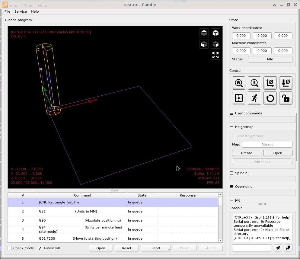


Loading the design
I start by loading the test.nc file generated with the checking software in the verification step. If you did not produce this file, you can use the edge cuts gcode file instead.
Probe Setup
If you are going to run a height map, which I recommend, you'll need to get probes setup. If you are unfamiliar with the concept, your CNC should have a couple of terminals where you can attach wires. On mine and many controllers, this is at port A5 on the controller. When these wires short together, the CNC firmware receives a signal which it will interpret as "contact" between the bit and the material. Because the bit and copper PCB are metal, they can participate in this electrical connection.
So you simply connect one probe to the bit and one to the board. To connect to the board, I take a little piece of wire that I clipped of from a resistor/capacitor/whatever of an old project and solder it to some upper corner of the board (I go upper left).
Zero X, Y
If you followed my method of putting the zero point in the upper left corner, you can zero the XY of the CNC machine just a bit under the soldered probe pad. Where you place the XY it is up to you so long as the cutting stays in the copper area and the bit doesn't crash into anything.
Zero Z
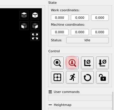
With the probes attached and the bit around 2mm above the copper, you should be able to test the "zero" feature of your CNC software (third image)
Tip: Doing a probe like this is a bit unnerving the first time as it will be the first end-to-end test of your setup. If you have an appropriate mechanical spring lying around, you can use it as your "bit" for testing purposes with your hand at the abort button in case the probe fails and the spring starts to compress.
Generating a Heightmap File


The z tolerance for a quality copper cut is tight. I'd say around 0.02 mm if you are going for 0.4mm wide traces and even tighter if you are going smaller.
To get this kind of precision, a height map will help immensely. The way a heightmap works is that it probes your board in a grid-like fashion, then alters the commands that will be sent to the CNC machine to conform to the collected data. The result is that you will see much better depth consistency.
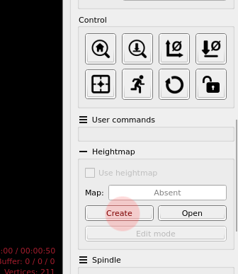
To generate a height map in Candle, you first click on the "Create" button under the "height map" section on the right. The bottom of the window changes to a setup UI.
Looking at the third image above:
- Click the autosize button to appropriately-size the probing area
- Pick a row and column count. More will result in a better height map in trade for more probing time. I think that a grid size of ~1cm is an acceptable starting point. In this case, the design was 21x21mm so I went with a 3x3 grid.
- There are also "interpolation settings". I always set these to the same values as the grid ones.
- Look everything over one final time and click "probe" when you are ready to commit. The machine will start to collect data. When it is done, you will see something like the 4th image.
- Go to the File menu and chose "save". I name my file `height.map`.
- Click the "Edit" button to get back out.
Now we look at the 4th image above:
- To actually use a heightmap click "Open"
- Make sure that the "use heightmap" option is checked. As you check and uncheck the option you should see the design slightly change, indicating that the heightmap data is being applied.
Calibrating the Heightmap (Optional?)


I found that for my 3018 machine, the height map process is precise but not accurate. Putting it another way, I'll see errors in the height map results of 0-0.15mm BUT this error is consistent across every point so simply shifting all of the points some fixed amount leads to a good result.
If your machine has this issue, below are two approaches for dealing with it.
The way I recommend is to generate a modified version of the heightmap. The tool, candle_heightmap_adjust.py is included in this project. Here is how I use it:
  $ python3 candle_heightmap_adjust.py --input height.map --offset 0.1
  Wrote height_offset0.1.map
This creates an new heightmap file with the requested offset applied. The first image above shows a before/after comparison of a modified heightmap file.
As you can see, the numbers were all simply shifted the requested offset.
An alternate approach is to manually rezero the machine slightly. This is only needed if you are not using candle_heightmap_adjust.py. Get the machine to z=0 somewhere off the PCB, then manually move the bit up the Z direction by 0.1mm. Then click "zero Z" to set the new zero point.
Now we can use the loaded test file to validate our depth (2nd image).
- Load the `heightmap_offset0.1.map` file into candle and make sure "use heightmap" is checked.
- Click "Send"
The machine will "cut" a rectangle outline which should only take a minute.
Maybe your bit never touched the copper. That's because we told it to cut at a height of 0.1mm (due to the heightmap file) above the board. If that is the case, try repeating with a `heightmap_offset0.05.map` file. e.g.
  $ python3 candle_heightmap_adjust.py --input height.map --offset 0.05
  Wrote height_offset0.05.map
and keep decreasing the height in 0.05mm steps until you finally see the bit make contact.
OR 0.1mm might be your perfect number, in which case you'll see the lightest of contact with the board, scratching the copper but not making it through.
OR 0.1mm might be cutting through to the copper. In this case, you'll want to make a 0.15mm file and probably go with it assuming the 0.1mm cuts were not too deep.
You might also find that the number you choose is inconsistent in places on the board (sometimes cutting sometimes not). This can happen if the board is of a lower quality and it not actually flat enough for your chosen grid to capture. If this is the case, you'll probably need to cut in multiple passes, each 0.05mm deeper, until all of your traces are good. This will keep your bit from breaking (as a result of cutting too deeply in one pass).
If it's really off, you can start over with more heightmap points, on a different part of the copper clad.
Cutting the Copper Traces

At this point, you should have a calibrated height.map file (be it the original, or one with an offset applied) and you are ready to cut for real.
Load your copper gcode and reload the heightmap (which Candle clears out when loading a gcode file).
Look everything over once more and start cutting!
When your cut is finished, vacuum the cut material away and inspect the board. It may be obvious that the bit did not cut deep enough everywhere. If this is the case, you can either:
- Rerun the candle_heightmap_adjust.py tool with a height 0.05mm lower, load it into candle and rerun the cut. Do not rezero the machine.
- OR Use the manual rezero Z trick described in the previous step to change the z zero point by 0.05mm
In some cases, you might need to recut incrementally more than once.
After you think the cuts are deep enough, you can sand the board. I use 400 grit first, then 1500 grit. It's not a long process, just a few seconds with each. I then use a paper towel with some isopropyl alcohol on it for a final clean.
Next consider getting out a multimeter and start poking around on the board, looking for unexpected shorts / opens.
Drilling Holes
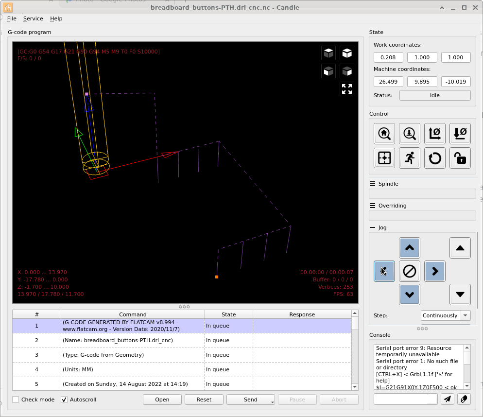
Drilling holes is easy compared to isolating traces. You just load a drill bit and rezero the Z axis. Do not rezero XY as this will mess up the drill locations. I zero Z using this "paper" method:
Get the bit within 2 mm of the surface, then set the Z increment to 0.1mm. Next, move a piece of paper between the bit and PCB while moving it down in 0.1mm increments. When the paper sticks, click the Z-zero button in Candle.
Note: You might think to use the probes to zero the drill bit. If you do so, make sure there is a conductive path to the bit as the isolation routing process may have isolated your board from the probe. I once broke a drill bit because I didn't think about that!
You can use the heightmap file here you if want to but it's not required as the need-for-z-precision is lower.
Watching the machine drill the holes so efficiently and precisely is one of the highlights of the process for me.
Board Cutout & Finishing Up
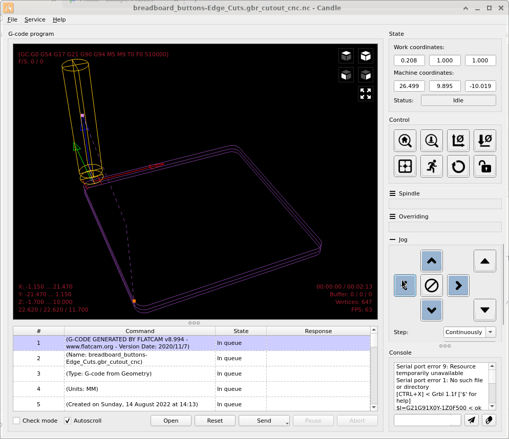


Compared to copper isolation, the board cutout is a relatively straight-forward task. Load up your endmill bit and z-zero it using the same paper technique as described in the drilling section.
Removing the board
Now that everything is done, you just need to dislodge the board. I get if off the surface by wedging in a flathead screwdriver and gently working at it on a side until it comes loose. Move the bit away in case something slips. I usually leave the rest of the PCB on the machine so I might have fewer steps to do on the next board I cut.
You are finished!
There were a lot of steps in this process but actually doing it doesn't seem too bad - a bit fun even. Good luck with the soldering!