STM32-Based Smart Home Hub
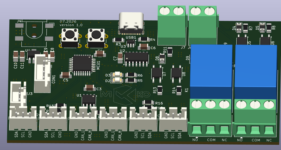
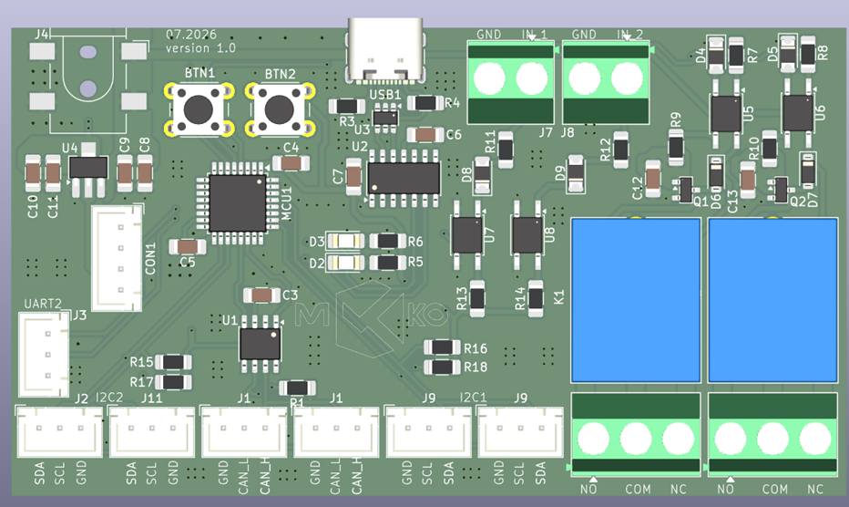
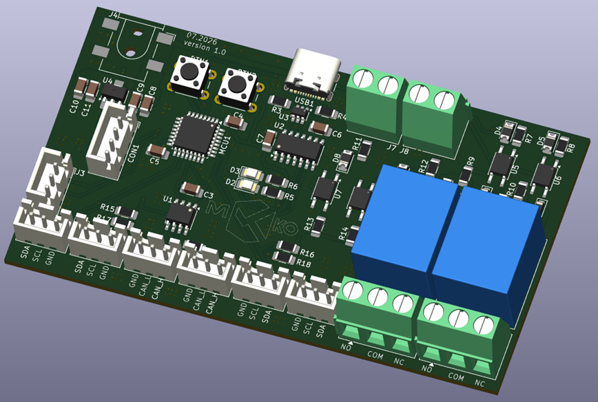
Most smart home controllers force a choice: either a closed commercial hub with a proprietary radio protocol and vendor lock-in, or a pile of cheap WiFi relay modules that turn a whole house into a congested wireless mesh with no real-time guarantees. This project takes a third path — a wired, CAN-bus-based system built entirely around a custom PCB.
At its core sits an STM32G431KBT6 handling all the real-time I/O locally — relay switching, digital inputs, CAN and I2C buses — while a Raspberry Pi 4 sits upstream over UART, running the management server and GUI. Every I/O boundary on the board — both relay outputs and both digital inputs — goes through optical isolation before it touches the MCU, and the board exposes CAN, dual I2C, and UART breakouts along its edge so it can act as the hub for a growing network of expansion boards.
In this Instructable, I'll walk through the design decisions behind this board: why build a custom wired system instead of using off-the-shelf smart home hardware, the reasoning behind the MCU and power choices, how the isolated I/O and CAN interface are built, and what's planned for the boards that will eventually hang off this one.
Why Build a Custom Controller Instead of Buying One?
Home automation already has plenty of mature options, so it's worth being upfront about where this board fits and where it doesn't.
Commercial closed hubs (Grenton CLU Z-Wave, Fibaro Home Center):
- Strength: turnkey, polished mobile apps, certified radio compliance, vendor support.
- Weakness: closed protocol and proprietary expansion modules at proprietary prices — the whole system's feature set is capped by what the vendor decides to sell, not by what's technically possible.
ESP32/ESP8266-based relay modules:
- Strength: dirt cheap, WiFi built into every node, huge community support through Home Assistant/ESPHome, fastest path from zero to "it works."
- Weakness: every node is an independent WiFi client — scale that to dozens of switches across a house and you get RF congestion, per-node firmware update overhead, and a control path that shares bandwidth and CPU time with the WiFi stack instead of running deterministically. There's also no natural way to wire a clean, isolated, multi-drop fieldbus between nodes; each device just talks to the router.
Raspberry Pi driving relays directly (Home Assistant + GPIO relay boards):
- Strength: one device, simple software stack, nothing to design.
- Weakness: Pi GPIOs aren't galvanically isolated from whatever they're switching, Linux isn't a real-time OS (a kernel update or filesystem hiccup can introduce switching jitter or a missed event), and the Pi becomes a single point of failure for the entire house's control layer.
This project's answer is a wired CAN-based fieldbus of STM32 nodes, with the Raspberry Pi sitting one layer up as the orchestration/GUI brain rather than the thing directly switching mains-adjacent loads. That buys hard real-time local control that keeps working even if the Pi reboots or hangs, proper isolation at every I/O boundary, and a bus topology that scales far more predictably than a house-filling WiFi mesh.
The honest trade-off: this is dramatically more work than flashing ESPHome onto a $5 module. Every I/O channel here needed its own isolation and driver circuit designed from scratch, and the multi-node CAN protocol still has to be written by hand — there's no Home Assistant integration waiting on the other end. Whether that trade-off is worth it depends entirely on the goal: "smart home working this weekend" is solidly a Home Assistant win, no contest. "Full ownership of the hardware and protocol for the long haul" is this project's actual goal, and that's the trade being made here.
System Architecture Overview
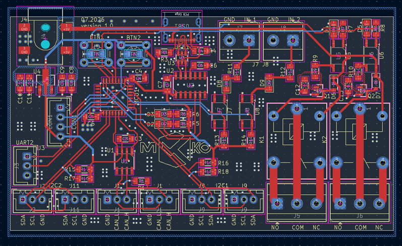
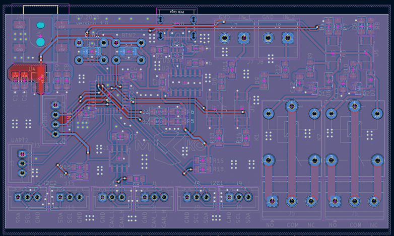
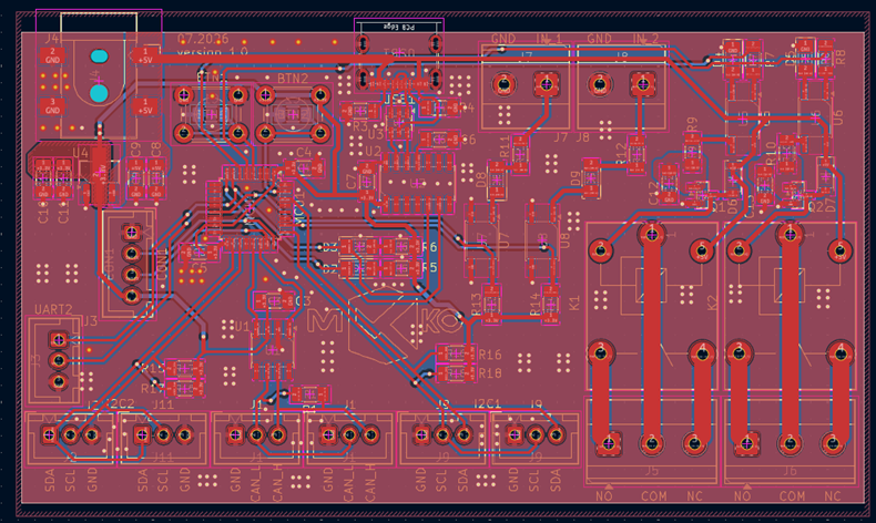
Before the schematic details, here's how this board fits into the larger system:
- STM32G431KBT6 (this board) — the "main" controller. Handles direct I/O: relay switching, digital inputs, and communicates upstream to the Raspberry Pi and, eventually, downstream to expansion boards over CAN.
- Raspberry Pi 4 — runs the management server and GUI, the layer the end user actually interacts with. Talks to this board over a dedicated UART connector.
- Future expansion boards — not part of this revision, but relevant context: additional relay-output boards and a sensor board are planned, joining this board's CAN bus as further nodes.
The Brain — STM32G431KBT6
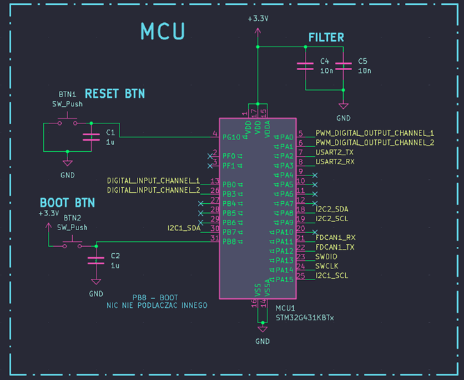
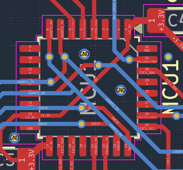
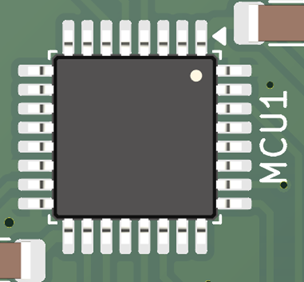
This board uses the same MCU family as my companion STM32G4 dev board project — a Cortex-M4 running at 170 MHz with hardware math accelerators. The reasoning for choosing it here carries over, with one addition specific to this application:
- Native FDCAN peripheral — this is the actual deciding factor for a multi-node fieldbus system. The G4 series has a full CAN controller built into the silicon, so joining the bus only costs one external transceiver chip (see the CAN section below), rather than needing an external CAN controller IC on top of the MCU.
- 170 MHz Cortex-M4 core — plenty of headroom to run isolated I/O handling, a CAN protocol stack, and UART communication to the Pi simultaneously without timing conflicts.
- Fast 12-bit ADCs, comparators, and op-amps on-die — not used by this first revision, but available for future features like current sensing on the relay outputs (load/fault detection) without needing an external ADC chip.
- CORDIC/FMAC hardware accelerators — overkill for pure relay switching today, but the same silicon leaves room for local signal processing (e.g., zero-cross detection for phase-controlled dimming) in a future revision without a chip swap.
Where it costs something compared to the "obvious" smart-home choice, ESP32: no built-in WiFi/Bluetooth radio. That's intentional here, not a gap — the CAN-and-UART wired architecture was chosen specifically to avoid per-node wireless congestion and keep switching timing deterministic. The trade-off is that this board is not usable standalone; it depends on the Raspberry Pi to provide the network-facing layer to the rest of the world.
Power Architecture
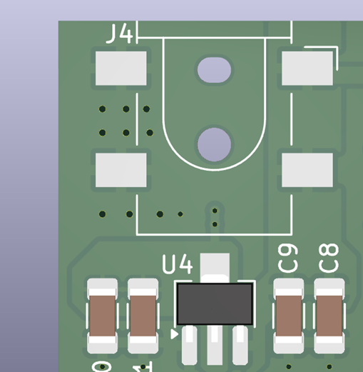
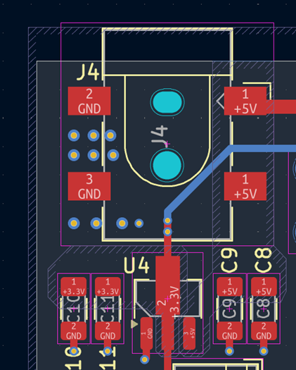
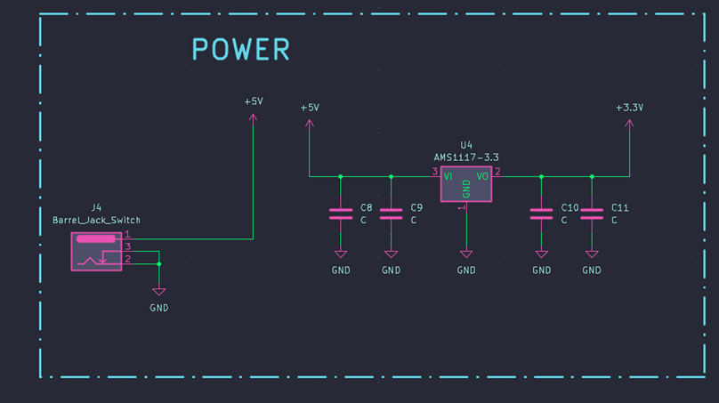
Power arrives at 5V through a DC barrel jack, then gets dropped to 3.3V logic level by an AMS1117-3.3 linear regulator (LDO).
Why an LDO makes sense here:
- Extremely simple — three pins and two capacitors, no inductor, no switching noise anywhere near the CAN transceiver or I2C lines.
- Negligible BOM cost, and the AMS1117's 1A rating is far more than this board's MCU-plus-peripherals load needs in practice.
Where the LDO approach costs you:
- All the dropped voltage (5V → 3.3V, roughly 1.7V across the load current) is wasted as heat rather than delivered as useful power. Efficiency tops out around 65–70%. Fine for a lightly loaded MCU-only rail — but as more 3.3V peripherals get added in future revisions (an RGB status LED, more sensors on the expansion buses), that heat budget stops being trivial.
- AMS1117 counterfeit parts are a well-known problem in the hobbyist PCB world. A large share of AMS1117 chips sold through generic/untraceable channels don't actually meet the datasheet's line and load regulation specs — a board can work fine on the bench with one reel and show a marginal, noisy 3.3V rail with a different batch from a different supplier. Worth sourcing from a reputable distributor rather than the cheapest listing.
A better alternative worth considering for a future revision: the AP2112K-3.3 (Diodes Inc., SOT-23-5) — smaller footprint, tighter output accuracy, built-in current limiting and thermal shutdown, similar unit cost, and far less commonly counterfeited than the AMS1117. For a logic-only rail that's about to pick up more peripherals across future revisions, this is the more future-proof choice.
Communication Interfaces


The left edge of the board breaks out every bus this system needs to talk to the rest of the house, each on its own small connector:
- UART (labeled UART2) — the dedicated, currently-active link to the Raspberry Pi 4.
- I2C2 — two breakout connectors, for local sensor/peripheral expansion.
- CAN — two breakout connectors (CAN_L/CAN_H), the bus this system's future expansion boards will join.
- I2C1 — two more breakout connectors, a second independent I2C bus.
On the top edge, two 2-pin screw terminals (IN1/IN2) bring in the digital inputs, and the two relay outputs get their own 3-pin screw terminals (NO/COM/NC) on the bottom edge — see Step 8.
Having two independent I2C buses rather than one is a deliberate bit of headroom: I2C address collisions between multiple similar sensor breakouts are a common annoyance, and splitting them across two buses from day one avoids that problem without needing an I2C multiplexer chip later.
Debug & Programming Interface — the MCP2221A USB-UART Bridge
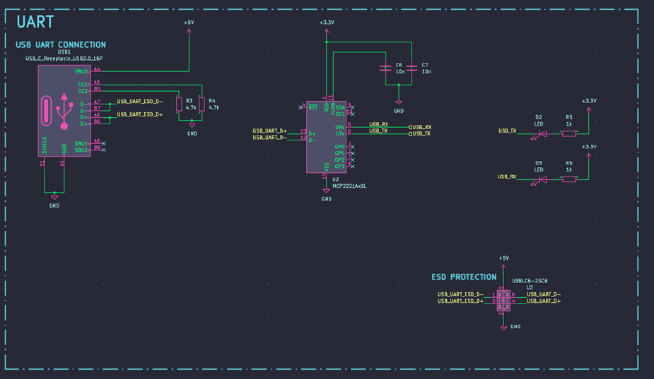
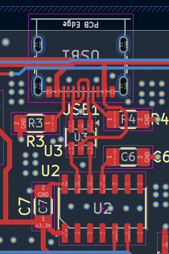
Like my STM32G4 dev board, this design uses Microchip's MCP2221A for the USB-C debug/config port rather than the usual CH340, CP2102, or FTDI FT231X.
Comparing the common options:
- CH340 — cheapest, but driver installation is often required and can be flaky on newer macOS; also one of the most commonly counterfeited USB-serial chips on the market.
- CP2102 — solid driver support, but usually still needs a separate driver install on Windows.
- FTDI FT231X — excellent throughput and driver maturity, but historically the most targeted chip for counterfeiting — to the point that FTDI's own drivers have in the past deliberately bricked non-genuine parts.
- MCP2221A — enumerates as a CDC device, using inbox drivers already present in Windows 10+, Linux, and macOS. No install step for the end user, plus a bonus onboard I2C master and GPIO/ADC/DAC lines that cost nothing extra in board space since the chip has to be there anyway.
The important trade-off specific to this board: the UART line feeding the MCP2221A bridge is the same physical UART used for the Raspberry Pi connector — not two separate channels. This is a real, deliberate simplification:
- Pro: saves a UART peripheral and two GPIO pins on an MCU with a limited number of USART instances.
- Con: the USB debug port and the Raspberry Pi cannot both actively drive the line at the same time — if both try to transmit, there's bus contention on TX. In practice, this means disconnecting or silencing one side while using the other.
For a first revision this keeps the board and BOM simple. If live debugging while the system is connected to the Pi becomes a real need later, the fix is a second dedicated USART (if a free peripheral/pins are available) or a UART mux/switch IC to select which device owns the line.
SWD Debug Header
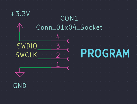
Alongside the UART bootloader path (via the MCP2221A bridge), the board includes a proper 4-pin SWD connector (CON1) on standard 2.54 mm pitch, carrying SWDIO, SWCLK, 3.3V, and GND.
Why having SWD at all matters: the STM32's built-in USART bootloader can flash firmware, but gives no breakpoints, no live variable inspection, and no fault register access. SWD is what lets a debugger step through code and actually diagnose a hard fault instead of guessing — the same reasoning that puts a real debug port on Nucleo and Discovery boards instead of relying on the bootloader alone.
A schematic note worth keeping as a "lesson learned": PB8 doubles as the BOOT0 selection pin on this package, and the schematic carries an explicit designer's note not to connect anything else to it — STM32 designs are notorious for silent boot failures when BOOT0 gets accidentally shared with another peripheral function.
What's missing compared to a full ARM debug connector, and why it's an acceptable trade here:
- No VTref/VCC sense pin, which a standard 10-pin Cortex Debug header includes so a probe can auto-detect the target's logic level. Omitted here because it isn't actually ambiguous — the board is hard-wired to 3.3V — but it does mean this connector needs a probe manually configured for 3.3V rather than plugging into a "universal" debug cable.
- Unshrouded 4-pin header risk — without a key or shroud, a cable can be seated reversed or offset by one pin, which on this pinout could short SWDIO to GND or backfeed the 3.3V rail. A clear pin-1 silkscreen marker is the mitigation here.
Suggestion for a future revision: a shrouded/keyed header, or — space permitting — expanding to 5 pins to add VTref, would make the board compatible with off-the-shelf ARM debug cables instead of a manually configured one.
Relay Outputs — With Optical Isolation
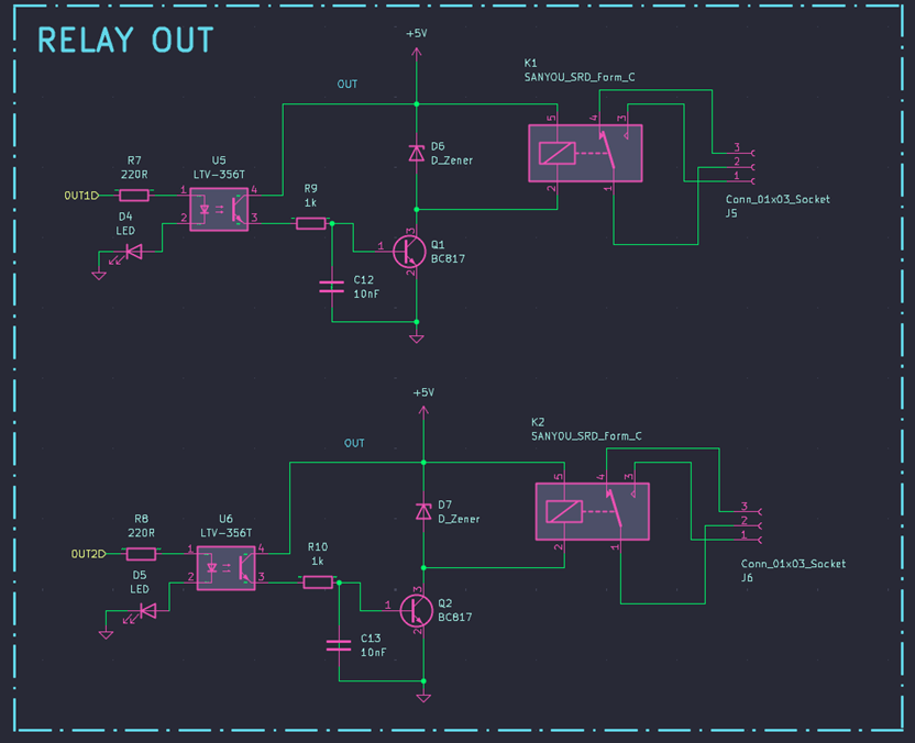
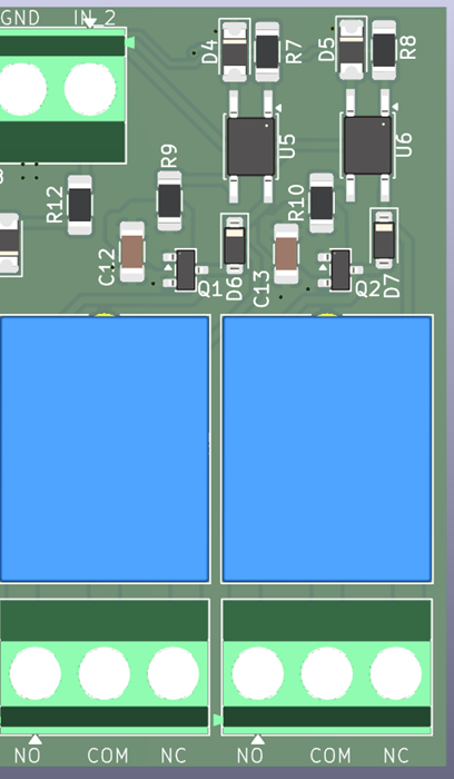
This is the part of the schematic worth highlighting as a genuine design strength: the two relay output channels aren't just "GPIO → transistor → relay." Each channel goes GPIO → LTV-356T optocoupler → BC817 transistor → relay coil, with a flyback protection diode across the coil, a snubber capacitor, and a dedicated status LED per channel. Each relay breaks out to its own 3-pin screw terminal (NO/COM/NC).
That optical isolation stage is a deliberate and valuable choice for a home automation board — it keeps the MCU's 3.3V logic domain galvanically separated from the relay-driving side, which matters given these relays will be switching mains-adjacent loads like lighting and sockets. It protects the MCU from switching transients, ground loops, and field-side wiring mistakes — a level of care many hobbyist relay boards skip entirely in favor of driving a relay coil straight off a GPIO-fed transistor with no isolation barrier at all.
Digital Inputs — Same Isolation Pattern
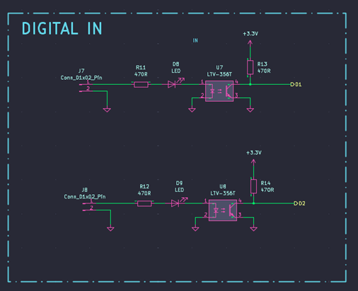
The two digital inputs mirror the output design: each goes through its own LTV-356T optocoupler before reaching the MCU, with a per-channel status LED, and its own 2-pin screw terminal (GND/IN). Same rationale as the outputs — isolating whatever external signal source (a physical wall switch, a door sensor, etc.) drives these inputs from the MCU's logic domain. Consistent, sound design across both I/O directions.
CAN Bus Interface
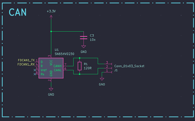
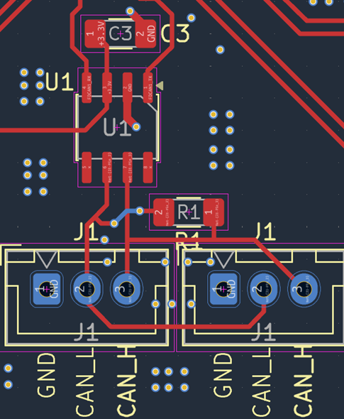
CAN connectivity is handled by a Texas Instruments SN65HVD230 — worth being precise: this is a CAN transceiver, not a CAN controller. The actual protocol engine (FDCAN peripheral) lives inside the STM32G431 itself; the SN65HVD230 only converts the MCU's logic-level FDCAN_TX/RX signals into differential CANH/CANL for the physical bus. It's a solid, widely-used choice — 3.3V native (no level shifting against the STM32 needed), low quiescent current, and a standard slope-control pin for tuning EMI vs. speed.
A 120Ω resistor provides bus termination on this board. Worth flagging for the planned multi-node expansion: 120Ω termination should only be populated at the two physical ends of a CAN bus, not on every node. If this main board always sits at one end of a linear bus topology, that's correct as-is — but once more CAN nodes join the chain, per-node termination needs to be reconsidered, since over-terminating drops bus impedance and degrades signal integrity.
Mechanical Form Factor
The board is designed for DIN rail mounting, keeping it consistent with standard electrical enclosure practice for whole-home installations — this is a controller meant to live inside a breaker panel or a dedicated automation cabinet, not sit exposed on a shelf.
What's Next
This is Revision 1, and the design is complete but still growing. A few things are already on the roadmap:
- A LAN port — not present on this revision; being considered for a future iteration.
- An RGB status indicator — currently there's no dedicated system-state LED beyond the per-channel I/O indicators; an RGB LED is being considered to communicate overall system state (idle, error, CAN activity) without checking logs on the Pi.
- Resolving the shared UART/USB contention — a second UART or a mux/switch IC to let the USB debug port and the Raspberry Pi link coexist without one having to be disconnected.
- Expansion boards over CAN — additional relay-output boards and a sensor board are planned to join this board's bus as further nodes. Still early concept stage and likely to change significantly before implementation, so more on that once the designs are further along.
As with my other STM32 projects, I'll document each revision as it happens — including what didn't work, since that's usually more useful than a polished final result.
Final Thoughts
This board isn't trying to compete with Shelly on price or with Grenton on polish — it's aimed at building a wired, isolated, real-time smart home backbone that isn't limited by what a vendor decides to sell, and isn't at the mercy of a house full of WiFi-congested relay modules.
The trade-offs are honest ones: an LDO that caps how much extra 3.3V hardware can be added before heat becomes a real concern, a debug header that assumes a fixed 3.3V target rather than supporting universal debug cables, and a shared UART line that means choosing between USB debugging and the live Pi connection at any given moment. None of these are design flaws so much as reasonable first-revision choices — and each has a clear, low-cost path to improvement (AP2112K regulator, keyed SWD header, a second UART) if and when it's needed.
For now, it does exactly what it set out to do: real-time, isolated I/O control at the heart of a growing wired smart home system — no cloud dependency, no vendor lock-in, and no wireless mesh to fight with.