The RP2040 Mini Board
.png)
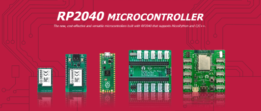
The electronic world is evolving to a complex and fascinating level. Manufacturers in these areas are coming up with more suitable and flexible components that are triggering advanced improvements in this area. The area of microcontrollers has not been left behind with more chips being pumped into the market. The RP2040 chip that has triggered more learning lessons in the area of automated home systems is already in the market. It is a product built by Raspberry Pi and it is in the long run fueling the microcontroller revolution triggering the rise of new platforms such as Arduino Nano RP2040 Connect, Raspberry Pi Pico, Wio RP2040 and so many others. Am going to document all you need to know about RP2040 where I will introduce it and list some projects, accessories, and products that can be built using the same microcontroller.
Supplies
.png)
KICAD
RP2040 Chip
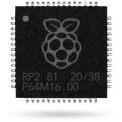
RP2040 chip
In February 2021, there was the introduction of the RP2040 into the market. The chip is built on dual-core Arm cortex-M0+ processors that are clocked at about 133MHz with an internal SRAM and an internal flash memory of 2MB and it can be coded in both C and C++ programming. It can also be programmed using the beginner’s MicroPython language. The chip has powerful hardware that can run machine learning frameworks such as the TensorFlow Lite.
Features of the RP2040
RP2040 caries around a noticeable signature of unique features such as ease of use, high performance, and relatively low cost. Besides very impressive technical values such as on-chip memory, rich peripherals, and a dual-core processor, the RP2040 chip can be coded with professionally preferred C++ and the beginner’s MicroPython programming languages.
With the chip, you are guaranteed high performance that is accompanied by low power consumption and extremely low leakage. You will note that it also has low power modes that help in extending its battery life. The feature makes the RP2040 suitable for applications that require a robust and longer use such as hobbyists and industrial use.
Another feature of the RP2040 is the programmable I/O subsystems which will provide more computing power to the users.
Below is the list of all the specifications of RP2040;
· Dual ARM Cortex-M0+ @ 133MHz
· Support up to 16MB off-chip Flash memory through a dedicated QSPI bus
· 264kByte on-chip SRAM located in independent banks
· Peripherals: 2SPI, 2 UARTs, 2 I2C Controllers, USB 1.1 Controller, 8 PIO State Machines, 16PWM
· DMA controller & Fully-connected AHB crossbar
· On-chip programmable LDO for generating a core voltage
· 2 on-chip PLLs for generating USB and core clocks
· Interpolator and integer divider peripherals
· 30 GPIO pins, where 4 are used for analog inputs
Using RP2040 to Design Mini Board
.png)
The next step is how to design the RP2040 MINI board and this design I did it perfectly on KiCAD EDA. The requirements for the projects are listed in the image below;
Drawing the Schematic in KiCAD
.png)
Drawing the Schematic In KiCAD
Open KiCAD and lay down all the components listed above and do the interconnection as shown below. Check of the electrical rules compliant is done. The addition of footprints is done at this level too then the schematic is annotated to give the components a unique identity for example if you have two capacitors one is labeled as C1 and the other C2. After annotation, the netlists are generated and the schematic pushed to the PCB layout stage.
PCB Layout
.png)
PCB Layout
After drawing the schematic, the next step is the PCB layout where the routing and even design of the 3D board are done. Here the size of the tracks on the board is calculated and determined. The 3D symbols and the footprints are confirmed to be in order. The edge cut is built up to define the size of the board. The board thickness is also confirmed at this level.
3D Output
.png)
After a successful layout process, the generation of the 3D view is done, and below is the outcome of the process.
The design is complete and what you need to do is to generate the fabrication files such as the Gerber files and upload them to your favorite manufacturer for the final manufacturing. You can generate the files from KICAD by hitting FILE then FABRICATION OUTPUT and generate all the files under this category from BOM, to DRILL files and others. Also, hit on FILE and then PLOT to generate the Gerber file which is also crucial in the design process.
How Is Fabrication Ordered?
.png)
.png)
.png)
How is Fabrication ordered?
Search PCBway then click on the Instant Quote page to get to the window shown below..
At this point, you need to start feeding in the necessary information so that you can have your design ready for an approximate quote.
Select the board type input the size of your board, select the quantity that you need, and the type of the material for the final board eg F4R, and finally the thickness a shown below.
Hit calculate to be fed with your approximate price for the board as shown below;
Hit submit to cart then you will end up with the pop-up window where you need to submit your Gerber files. Just submit the GERBER files then wait for the engineers to give you the final quote for the job and after you make the payment, you will get the finished product within seven days.