The World's Smallest Prototyping Board
by Piffpaffpoltrie in Circuits > Electronics
2076 Views, 7 Favorites, 0 Comments
The World's Smallest Prototyping Board

In this Instrucable I suggest a way to match a tiny SO-23 chip to a PCB designed for a TO-92 footprint.
The picture above shows one of my home-brew matrix board adapters with an SO-23 chip, in action on a populated and soldered PCB. In the background, a standard TO-92 transistor can be partly seen, too.
The Task
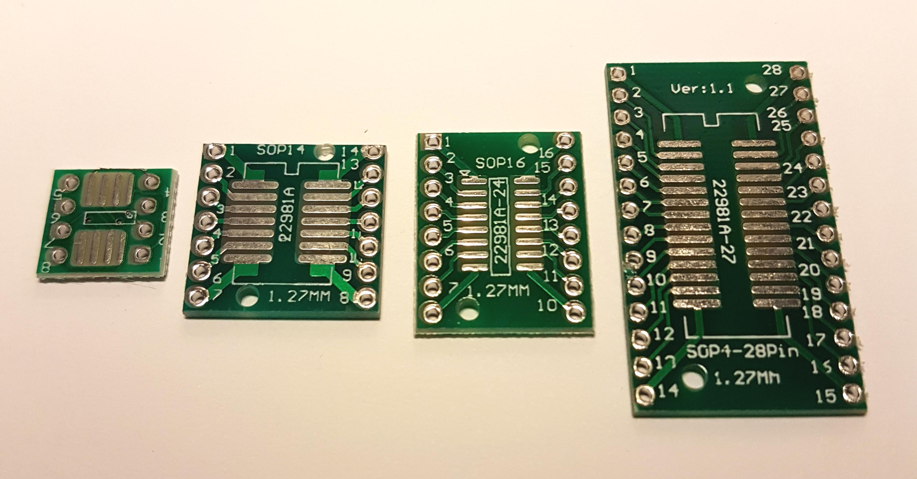


Soldering SMD (Surface Mounted Devices) chips with two, three or multiple terminals on a PCB is a minor challenge.
Replacing an IC in the standard DIL (Dual-In-Line) package by its tiny SMD equivalent - just because the DIL package was considered obsolete by the manufacturers and cannot be supplied anymore - is, in principle, an easy task: For the variety of 8, 14 or more pins, our friends from AliExpress, Banggood (or similar) supply adapter PCBs for little money (search term 'SMD adapter'). Since the shipment from China takes some time, purchasing and stocking some of them before you actually need them seems a good idea to me.
Carefully solder your SMD chip on one of these, install 'pins' using either some bare wire or multi-pin headers - and voilà!
Above, you can see some of these adapters - naked, as they are delivered, and after SMD chips and pins have been installed.
Going Smaller Now

But how do you get yourself out of it if you have a PCB that requires a 3-terminal component in the TO-92 (or even the old-fashioned TO-18) package, but then only an SO-23 SMD device is available?
In connection with a recent project I tripped over this exact problem: The BOM asked for a LM4041DIZ-ADJ reference voltage source in the TO-92 package, and the PCB was designed for its footprint as well. However, my usual purveyor to the house and the court did not stock it, but only had the LM4041CIM3-ADJ available, i.e., the SMD version in the tiny SO-23 package.
What to do? spake Zeus.
Above, btw, is a comparison of a TO-92 package next to an SO-23 package - and an Euro Cent as a token of scale.
My Idea
I didn't want to mess around with the (very nicely made) PCB. So I tried to produce a kind of adapter PCB from a leftover piece of prototyping board, aka perf board or matrix board.
BTW, I don't remember having seen any design of a 2x2 matrix board before (which is, in fact, a square of only about 5x5mm).
And, in my opinion, this is the smallest sensible size for a matrix board. Smaller ones, i.e. 2x1 or 1x1, with two solder pads or even only one, might be thought of. But these are neither particularly useful nor do they make any sense.
Preliminary Study

In order to check whether it is at all possible to place an SO-23 chip correctly on my piece of matrix board, I first produced a drawing blown-up ten-fold, that is, to 1000% (fig. 1), proving that my idea might work. BTW: If you want to do a similar thing yourself, you can easily find the dimensions of SMD components in the corresponding data sheets from the manufacturers.
Preparatory Work
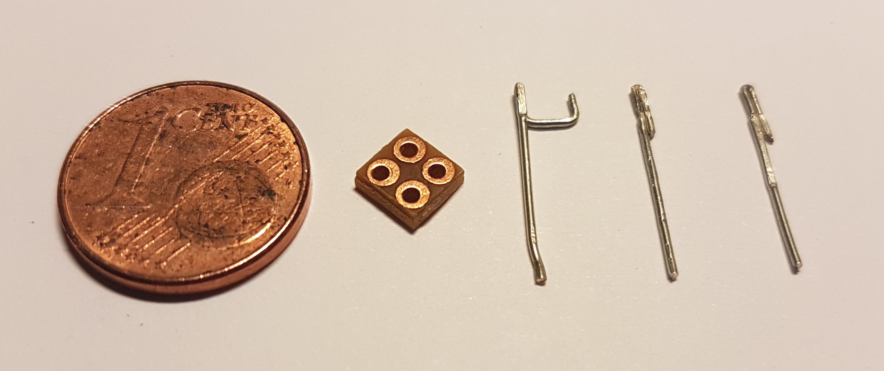
A single-sided matrix board cutoff is sufficient if you use it with its solder pads ('donuts') pointing upwards. Fix three 'terminals' consisting of bare, tinned copper wires of about 0.6 mm diameter in the corresponding holes. Before inserting them, bend their ends by 180° and flatten them slightly with a pair of flat-nose pliers, so that they snugly fit into the holes of the board without dropping out. In order for these terminals to match the footprint of the TO-92 device, the one in the top center must continue from the 'upper' pad to the one diagonally opposite, i.e. the 'lower' one (from north to south, as shown in red in fig. 1).
When soldering the terminals to the pads of the matrix board, a little vice comes in quite handy - just clamp all three terminals. Don't use too much solder when doing this, otherwise positioning the chip might become difficult later.
Realisation


While your assembly is still clamped in the vice, the SO-23 chip can be positioned and soldered. I admit that this is easier said than done, but I usually manage it at the 5th or 6th attempt...
It requires tweezers, a magnifying glass (preferably a watchmaker's loupe) and a very narrow soldering tip.
Sneezing or coughing while doing this is strongly advised against!
When you solder the chip, the tin with which the three terminal wires are connected to the solder pads melts again, and therefore it is quite convenient that the wires are somewhat fixed, both within their holes and in the vice.
DO NOT heat the chip's tiny terminals for longer than two to three seconds in order to avoid damage! Take a short break after each solder joint, allowing the pins to cool down.
(The pictures above show the assembly before and after soldering the pins, and after placing and soldering the SO-23 chip).
Further Applications?


In a similar way, but with a different arrangement of the SO-23 chip, also SMD transistors can be converted to the wired, TO-18- or TO-92-like version (fig. 2).
This application, however, only makes sense on weekends - when your friendly neighbourhood electronics shop is already closed and you urgently need a wired transistor, but you only can find an SO-23 type in your junk box (if you can find it at all).
If you install the SMD transistor upside down (that is, its label side down and its belly up) onto the adapter, you can even do without the diagonal feed-through. This way, the fourth - now obsolete - solder pad can be partially cut or filed off, and the shape of the little board, with some imagination, even approaches the outline of the TO-92 package (fig. 3).
Caution
Be aware of the fact that not all TO-92 transistors, even of the same type (as well as their SMD counterparts) have the same pinout - before proceeding, consult the data sheet and make sure that you do it right from the beginning.