Transcranial Electrical Stimulator, Arduino Compatible
by quicksilv3rflash in Workshop > Science
27210 Views, 68 Favorites, 0 Comments
Transcranial Electrical Stimulator, Arduino Compatible
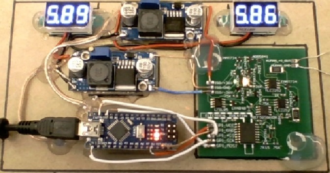


I've also written (much simpler) instructions for a tDCS-only device that you can build yourself, with just common through-hole parts, made a more advanced two-channel tACS device, and I've set up a preorder page for repetitive transcranial magnetic stimulation machines! ^.^
------
This device is an open-source replacement* for STARSTIM tCS, which is sold only to research institutions. I have not been able to get a price quote for this commercial tCS hardware because I am not an institution, but random people on reddit say it costs $10,000 to $25,000 for the full Neurostar tCS hardware. Point is, this transcranial electrical stimulator hardware design is open source, freely available to all of you and costs about $100 in parts ($95.09 as of early 2017).
If all you want to do is build, test, and use this device with the GUI I've written, you don't need to read the step "Here Be Dragons" or any of the steps after it.
This device can be used for any kind of human electrical stimulation, such as tDCS, tACS, tRNS, or tVNS. Its hardware, when properly constructed and tested, limits output current such that -2.1mA < output_current < +2.1mA , based on the 2mA safety limit recommended in these published guidelines.
*This device is only single channel, but this device can be stacked in parallel with itself without any additional circuitry to create a multichannel device with any number of channels desired at about $100 each. The driver code on the computer side will become hairier as you add channels, though. This device has four times the maximum output frequency of the STARSTIM tCS device, and comparable accuracy and DAC step resolution.
DISCLAIMER: This Instructable is posted for educational purposes only. This device may require permission from state-officiated medical personnel to officially use in your slice of the world, and can kill the user if improperly assembled and used without testing/verifying correct operation prior to use on humans. Do not use if you have a history of seizures, the author is not liable for seizures, headaches, undesired mental changes, insanity, reduced well-being of any kind ... mumble mumble... immolation and/or dismemberment and/or death ... mumble mumble ... void where prohibited ... this statement has not been evaluated by the Food and Drug Administration. This product is not intended to diagnose, treat, cure, or prevent any disease. But you should definitely look into the studies using transcranial electrical stimulation to treat depression.
Hopefully this is the last tES (transcranial electrical stimulation) device design I post for a while, because I don't see myself running into the hardware limitations of this one for a long time. With an Arduino as the SPI signal source, and the firmware posted here on github, it's limited to about 1kHz max output frequency, but with a higher-speed SPI signal source the device can go up to 30kHz full-swing, so this board should be good enough to replicate the stimulation pattern in almost all tACS/tDCS/tRNS studies published to date. I'd say "all" but I'm sure there were some jokers putting >30kHz into human heads for some reason. If >30kHz is required, it's relatively simple to swap a higher-frequency op-amp for the TLC2252. We humans top out at around 150Hz, as far as I know, so 30kHz should be plenty of bandwidth for injecting signals into us.
This device is designed with safety in mind. The data input (USB, which may be earth grounded/line powered) is electrically isolated from the power supply and output to the human (which is floating/battery powered) in order to prevent ground loops. Also, the hardware limits the output current to safe levels, +/-2.1mA, based on the safety limits defined in work at the University of Gottingen, the "Gottingen protocols", which among other things specify output current limited to "currents of 1 – 2 mA applied for durations up to 20 minutes". In the event of primary regulator failure, current is limited to +/-4.0mA by the backup safety resistors (in series with the typical ~4.7kOhm resistance of a human head with electrodes).
Interface: 3-wire SPI (16 bits per DAC write, no MISO pin, SPI mode 1, CPOL=0, CPHA=1, MSB first)
Precision: Max offset error +/- 15uA (much of this is a result of fixed offsets, e.g. resistor tolerances, that can be calibrated out if desired, but some is temperature dependent. This value was calculated by analyzing the circuit with worst-case offsets published in component datasheets, error values which lump both manufacturing offset and temperature-dependent effects)
Precision: DAC step size 1.1uA
Maximum output current: +2.1mA by design, prototype measures +2.08 mA
Minimum output current: -2.1mA by design, prototype measures -2.09mA
Maximum output frequency of tES circuit board itself: 30kHz (limited by full-swing amplification bandwidth of TLC2252)
Maximum output frequency of prototype: 976.5625 Hz, 512us per sample (using USB > Arduino nano as SPI data source, with 1.953125kHz output sample rate)
Maximum SPI clock input frequency of tES circuit board itself: 50MHz
Isolation voltage rating: 5kV
Downloads
Parts List

{{{{ Total cost: $95.09 }}}}
(prices as of early 2017)
$27.89 // printed circuit board
$28.16 // board components
$08.31 // device power components
$17.39 // human input components
$03.46 // data input components (YOUR [arduino / microcontroller / raspberry_pi / any_SPI_master_device] HERE)
$09.88 // device case components
===============================
Section 1: Components to populate the board (Total: $28.16, prices as of 2017-01-15, subtotal $23.17, $4.99 economy shipping)
--------------------------------------------------------
These are all from the same supplier, and I've linked directly to their product pages. You just need to open the links one by one and order the listed quantity. Get extras of the cheap ones if you suspect a tweezer mishap may send a tiny piece irrevocably flying off into shag carpeting... or you'll have to wait another week and pay double shipping. If you're feeling skilled, careful, and/or lucky, order exactly the required number of each piece.
$0.19/ea. 1x LG Q396-PS-35
$0.21/ea. 1x 150120AS75000
$0.55/ea. 3x FMMT734TA
$0.55/ea. 3x FMMT634TA
$1.03/ea. 1x ADR5041BKSZ-REEL7 (if out of stock, substitute ADR5041BKSZ-R2 at $1.41/ea.)
$0.10/ea. 6x CRCW060375K0FKEA
$0.09/ea. 2x ERJ-3GEYJ363V
$1.37/ea. 2x RG1608N-102-P-T1
$0.63/ea. 1x ERA-3AEB86R6V
$0.10/ea. 2x CRCW06037K15FKEA
$1.61/ea. 2x TLC2252CDR
$0.67/ea. 2x LM4040D10IDBZR
$2.98/ea. 1x REF5050AIDR (if out of stock, substitute REF5050AQDRQ1 at $3.51/ea.)
$0.39/ea. 1x L78L05ACD13TR
$2.76/ea. 1x SI8630BD-B-IS
$2.52/ea. 1x DAC7311IDCKR (if out of stock, substitute DAC7311IDCKT at $2.74/ea.)
$0.10/ea. 2x 35202K2JT
$0.17/ea. 4x GRM188R61H105KAALD
==================================
Section 2: the board itself (Total: $27.89 minimum, price as of 2017-01-19, SHIPPING RATES WILL VARY OVER TIME, $9.90 subtotal + $17.99 cheapest shipping)
--------------------------------------------------------
The .zip file provided is compiled for SeeedStudio Fusion PCB specifically! You'll need to go to the github repository [LINK TO ASSOCIATED GITHUB REPOSITORY] to get the actual .brd files and reprocess them if you need gerbers (PCB design files) for a different manufacturing service. I'm only giving instructions for purchasing though Seeed here because they're the service I used for the tested prototypes, and also the cheapest I've found that doesn't noticeably cut quality.
Ordering instructions:
You'll be ordering from SeeedStudio Fusion PCB. These people have a two-week maximum manufacturing turnaround time but a really slow shipping carrier (if you select the cheapest shipping option, estimate 3-5 weeks to get your boards) and you have to make an account to order from them, which is annoying.
(CHEAP / FAST / HIGH-QUALITY < one can choose any combination of two of these three. Seeed is CHEAP and HIGH-QUALITY.)
After making an account with SeeedStudio (sorry), you need to submit a set of gerber files to be manufactured, packaged in a .zip. I've already assembled the .zip for you, it's embedded at the bottom this step, seeed_fusionpcb_gerber.zip. Download it. This .zip file is also on github.
On the order page linked, click the button labeled "Add your gerber file", browse to your downloaded copy of seeed_fusionpcb_gerber.zip, and upload it.
Select the following options:
MATERIAL: FR4-TG130 (or whatever says FR4 as the first three characters)
LAYERS: 2 LAYERS
DIMENSIONS: (manually enter or click the blue autofill measurements to the right of "DIMENSIONS") 56.5 * 56.5 (mm)
PCB QTY: 10 (might as well, there's no price break for 5...)
PANELIZED PCBS: 1
PCB THICKNESS: 1.6 (mm)
PCB COLOR: GREEN (you can choose a different one but they charge more)
SURFACE FINISH: HASL
COPPER WEIGHT: 1 OZ.
MIN HOLE SIZE: 0.3mm
MIN TRACKING/SPACING: 6/6 mil
BLIND VIAS: NO
HALF-CUT/CASTELLATED HOLES: NO
IMPEDANCE CONTROL: NO
...then click "add to cart", and then the little cart icon in the top-right, and then it's a standard online retailer checkout.
It's highly recommended to get expedited shipping.
(Isn't ordering boards fun? Look at all the miscellaneous units up there! Ounces (per square foot, implicitly), millimeters, mils... why choose between the imperial and metric system when you could make an even more convoluted global standard setup that drags in units from both?)
===============================
Section 3: device power components (Total: $8.31, from various suppliers around ebay as of 2017-01-18)
These device power supply components are standard blocks that have been cloned by multiple suppliers. They're cheap, common, identical from multiple manufacturers and sellers, and they appear reliable (never had one break yet), but I can't find the "proper" names and model numbers for them. So I've linked ebay search results instead of specific product pages.
--------------------------------------------------------
$1.68/ea. 2x "DC 3-32V Step Up to 5-35V Boost Converter Voltage Regulator Power Supply Module"
$0.99/ea. 2x "Mini DC2.5-30V LED Panel Voltage Meter 3-Digital Display Voltmeter"
$0.99/ea. 2x "Holder Case For 4AA (6V) With Wire Leads Plastic Battery Storage Box"
$0.99/ea. 1x "DPDT ON/ON Toggle Switch"
===============================
Section 4: human input components (Total: $17.39, from various suppliers around ebay as of 2017-01-18)
The searches linked in this section should pull up 2mm pin connector leads and 2mm pin compatible sponge electrodes. IF YOU WANT TO USE "AMREX" STYLE SPONGE ELECTRODES YOU NEED "BANANA PLUG" LEADS INSTEAD OF 2mm PIN LEADS!
--------------------------------------------------------
$15.50/ea. 1x "tDCS Dual Electrodes bundle: Sponge (1pair) & Self-Adhering (2pair)"
$01.89/ea. 1x "Standard Electrode Lead Wires Standard Pin Connection For Tens / Ems Machines"
===============================
Section 5: data input components (Total: $3.46, from various suppliers around ebay as of 2017-01-18)
--------------------------------------------------------
$2.70/ea. 1x "MINI USB Nano V3.0 ATmega328P CH340G 5V 16M Micro-controller board Arduino"
$0.76/ea. 1x "Hi-Speed 80cm USB 2.0 Male A to Mini B 5-pin Charging Cable Hot-swappable LF"
===============================
Section 6: device case components (Total: $9.88 from home depot as of 2017-03-07)
--------------------------------------------------------
$3.72/ea. 1x 61cm x 61cm x 6mm Medium Density Fiberboard
$1.98/ea. 2x 2cm x 2cm x 91.5cm Hardwood Square
$4.18/ea. 1x 20cm x 25cm x 2.4mm Lexan
===============================
Downloads
Power Supply Assembly and Testing

WHENEVER I SAY GLUE I MEAN HOT-MELT GLUE!
I am using hot-melt glue to hold this entire device together. Hot-melt glue is nonconductive, gap filling, and possible to remove for rework with a heat gun. All of the modules in this device have different sizes of mounting holes, and gluing them down is much easier than specifying 4 different sizes of screw and pilot hole.
[ -- Used in step -- ]
Hot-melt glue
Solder
Stranded wire pair, 24ga
Solid wire, 22ga
1x DPDT switch
2x 4AA battery holder
2x boost regulator
2x digital panel meter
1x (203mm x 132mm x 5mm) medium-density fiberboard (MDF)
1x (203mm x 20mm x 20mm) square dowel
2x (90mm x 20mm x 20mm) square dowel
2x (85mm x 20mm x 20mm) square dowel, required_length is given by the equation:
required_length = (203mm - your switch length in mm) / 2
[ -- Procedure -- ]
Glue the five pieces of dowel and the switch to the medium-density fiberboard (MDF) as shown. Roughen the backs of the battery holders and the corresponding location on the MDF with sandpaper, then wipe the rough spots clean with dry paper towel or cloth. These mating surfaces require roughening because the glue joint will be subjected to extra stess when batteries are inserted or removed. Use hot-melt glue to adhere the battery holders to the MDF as shown.
Align the device with the battery holders directly facing you and the switch pointed up, and drill a 5mm hole in the middle of the space above the battery holder on the left. This hole does not need to be precisely located. Draw a border line on the MDF, on the side opposite the battery holders, 20mm in from the edge of the board. Keep parts, wires, and glue inside this border line.
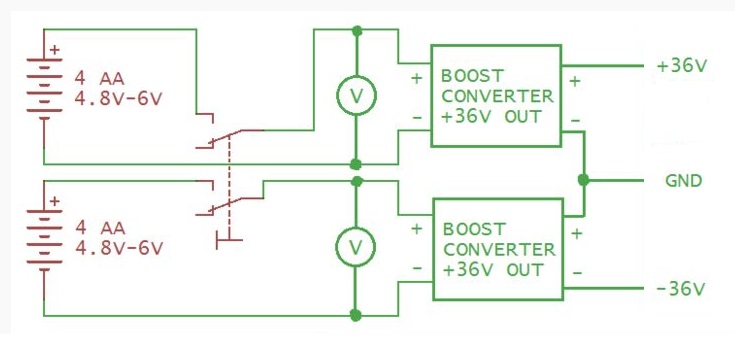
Run wires from the battery packs to the switch, as shown in the schematic, and then through the hole to the top of the board. Solder all joints. Glue wires in place, sealing the hole.
Set the device down with the switch and battery holders facing down. Glue the panel meters to the top of the device, as shown. Twist (but don't solder, yet) the leads from each panel meter to the plus and minus of the correct wire pair, that is, the one from the battery holder directly below it.
[ --- TEST STEP --- ]
Put batteries in one of the holders. Turn on the switch and verify that the panel meter above this holder illuminates. Turn off the switch and verify that the panel meter turns off. Move the batteries to the other holder and repeat this process for the other meter.
If the test above is passed, remove all batteries and solder the twisted wires. Glue the boost converters to the MDF, as shown. Melt extra solder onto the IN+ and IN- pads of each boost converter. For each boost converter input terminal, liquify this extra solder and melt the soldered twisted pair from the battery holder / panel meter into it. It does not matter which boost converter each battery holder connects to, as long as both the + and - from each battery holder go to the same converter.
[ --- TUNE STEP --- ]
Put batteries in both holders. Turn the device on. Measure the output voltage of one of the boost converters with a multimeter, and adjust the potentiometer (with a tiny screwdriver) until the output voltage is 36V. Repeat this process with the other boost converter.
Solder the boost converters together in series and run wire to where the board will be placed, as shown in the picture.
Adding Arduino for Data Input


Glue the Arduino Nano to the MDF in the position and orientation shown above. Solder wires to the following pins:
D10
D11
D13
5V
GND
These wires will later be soldered to the tES device board:
D10 > SPI_*CS
D11 > SPI_MOSI
D13 > SPI_SCK
5V > SPI_VCC
GND > SPI_GND
Soldering the Board

This board might look intimidating if you haven't done much SMD soldering work, but it's not actually that hard*, so don't worry! Here's a guide to SMD soldering, also attached at the bottom of this step.
*As long as your iron is temperature controlled, you get pretty much infinite do-overs. You *will* bridge the pins, unless you're this person, and that's OK! Simply remove the solder bridges with a desoldering braid afterwards.
All LEDs are aligned cathode down, and all chips with 6 or more pins are aligned with pin 1 in the top left, in the view shown above. Everything else's alignment is either obvious (3 pins and only fits one way) or doesn't matter (resistors and nonpolarized ceramic capacitors). I designed this board with ease of building in mind.
[ -- Used in step -- ]
Temperature controlled soldering iron (recommendation for Sn/Pb solder: set to 320 C for soldering, 375 C for desoldering with the desoldering braid)
Flux pen
Desoldering braid
Tweezers
60/40 or 63/37 Sn/Pb solder, fine diameter, rosin core
Circuit boards and tiny components previously ordered from Mouser and Seeed
[ -- Procedure -- ]
Your soldering process for multipin surface mount chips will look like this:
1. Use flux pen to coat pads on board
2. Blob solder on a corner pad
3. Grab chip with tweezers and align on circuit board pads while holding iron tip to the corner pad that got extra solder
4. Remove soldering iron tip, check chip/pad alignment, GOTO 3 if chip is misaligned
5. Melt solder into the general vicinity of the pins/pads. Some pins will probably be bridged.
6. Raise iron temperature, remove solder bridges with desoldering braid
7. Reexamine solder joints for bridging, GOTO 5 if bridged (adding a little solder to a bridge so it's convex makes it easier to remove with the desoldering braid)
Downloads
Connecting Power Supply and Data Input

[ -- Used in step -- ]
Hot-melt glue
Solder, rosin core
Solid wire, 22ga
tES device board, populated
1/4w 1kOhm resistor with wire leads
[ -- Procedure -- ]
Glue the tES device board to the MDF.
PRESERVE OUTPUT ELECTRICAL ISOLATION! DO NOT CONNECT SPI_GND TO ISO/GND OR HUMAN_GND!!
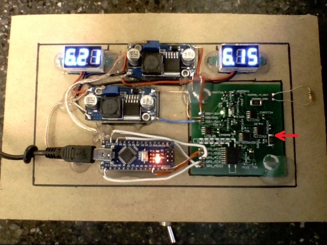
Solder ISO/+36V, ISO/GND, and ISO/-36V lines from the boost converters to the corresponding pads on the tES device board. Solder SPI_VCC, SPI_GND, SPI_*CS, SPI_SCK, and SPI_MOSI lines from the Arduino to the corresponding pads on the tES device board. Solder the 1kOhm resistor across HUMAN_+I_OUT and HUMAN_GND as shown. This resistor is used for testing the device. It's very important to test the device before connecting it to anyone's head. I shouldn't have to tell you that, but I'll say it again louder just to make sure:
IT'S VERY IMPORTANT TO TEST THE DEVICE BEFORE CONNECTING IT TO ANYONE'S HEAD!
PRESERVE OUTPUT ELECTRICAL ISOLATION! DO NOT CONNECT SPI_GND TO ISO/GND OR HUMAN_GND!!
[ -- Test steps -- ]
With the device off, measure the resistance between the HUMAN_+I_OUT pad and the top solder joint of the 2.2kOhm resistor on the bottom right (see red arrow in the above picture). This resistance should be between 4.18kOhm and 4.62kOhm.
Turn the device power switch on. The green LED on the tES device board should illuminate. Measure the voltage between HUMAN_+I_OUT and HUMAN_GND (across the 1kOhm test resistor). This voltage should have a magnitude of less than 10mV (it measures -0.5mV on my device).
Turn the device off again. Just to make sure, measure the resistance (again) between the HUMAN_+I_OUT pad
and the top solder joint of the 2.2kOhm resistor on the bottom right (see red arrow in the above picture). This resistance should be between 4.18kOhm and 4.62kOhm. This test is repeated because those resistors are a critical safety system.
Software and Firmware

Install the following software on your computer:
Pygame 1.9.2pre (I'm using pygame-1.9.2a0.win32-py3.2.msi)
The versions listed above are somewhat out of date. I am linking to them because they are the versions I used to write and test the device's driver software, and I while the driver software should work with up-to-date versions of the above programs, I cannot guarantee that it actually will.
Instructions to install Python and PySerial
Alternate instructions to install PySerial
Instructions to install PyGame
Plug the Arduino Nano into a USB port and start the Arduino development environment.Go to Tools > Port, and see which port the Arduino is connected to. This port will vary depending on which OS your computer has, and which specific USB port on your computer the Arduino is connected to. The other settings in the Tools menu should be: Board type: Arduino Nano, Processor type: ATmega328, Progammer: AVRISP mkII.
In the Arduino IDE, load FINAL_BUFFER_DAC7311, which is linked on github here, and also embedded at the bottom of this step. Press Ctrl+R, wait for the Arduino IDE to report "the sketch uses X% of the program memory space" and then press Ctrl+U. Wait for the green "loading bar" to finish its progress. In the Arduino IDE, open the serial monitor (Tools > serial monitor). When set to 115200 baud and the correct serial port location, the serial monitor should show "ÿÿÿÿÿÿÿ" forever. The program on the Arduino is sending 0xFF over and over, because its buffer is empty and it's requesting data to fill it. The hex code 0xFF might render as something different on your system, on mine it's a lowercase letter y with an umlaut. At this point the firmware is loaded and good to go!
Open IDLE. IDLE will have been installed with Python as your default Python IDE. Within IDLE, type "import pygame" and press enter. If you see "ImportError", you need to figure out if you've got incompatible version numbers of Python and PyGame, and go through the install process for each one again, but more carefully. Google and StackExchange can help you do this. If you DON'T see "ImportError", you're golden. Type "help(pygame)", press enter, and verify that a huge wall of text (that you don't need to read) appears. Next, type "import serial", press enter, verify there isn't an ImportError, type "help(serial)", press enter, and verify that another wall of text appears. If "import serial" fails, you need to look at your PySerial installation and verify you have compatible version numbers and that you properly followed the installation instructions. Close IDLE.
Run the python script KludgeGUI. A console window will appear, asking you for the serial port location. On my setup, this location (shown in the Arduino IDE under menu Tools > Port) is called COM6, so I type in COM6 and press enter. A second window will appear over the console window, a graphical interface, named "tES device control program". This is the GUI to control the device. Everything [IN BRACKETS] in the GUI is a clickable button that changes the output. The output waveform is shown in the GUI. If you increase the frequency, the waveform image in the GUI will become more like a set of stairs than a smooth curve. This is not an error in the GUI, the distortions shown in the GUI match the output waveform (as seen with an oscilloscope) very closely.
[ -- Test step -- ]
After connecting the device, with the device power switch on, open KludgeGUI and verify that the device's amber LED turns on, and the RX and TX LEDs on the Arduino become active. Measure the output voltage across the test resistor. The voltage across the 1kOhm test resistor should measure <10 mV in magnitude, on my system the measured value is -0.8mV.
Testing and Verification

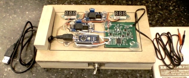
Turn the device on, but do not connect it to the computer yet. Verify that the green LED on the tES device board turns on but the amber one does not (the amber LED might briefly flash during device turn-on, which is ok). Measure the output voltage across the 1kOhm test resistor, it should be less than 10mV in magnitude (-0.5mV on my device).
Plug the tES device into your computer and use the Arduino IDE to find out which serial (called COMsomething on windows, /dev/tty.something on mac) port it is connected to. Launch KludgeGUI and enter the appropriate serial port. The RX and TX LEDs on the Arduino should become active, and the amber LED on the tES device circuit board should illuminate. Measure the output voltage across the 1kOhm test resistor again, it should be less than 10mV in magnitude (-0.8mV on my device).
Perform final tuning on the boost converters. With the device connected and on, and KludgeGUI running, and after verifying that the device's amber LED is on, measure the output voltage of each boost converter and turn the set-screw on each boost converter until their output voltages measure 36.0V. You may use hot-glue to fix the position of the tuning potentiometers on the boost converters after doing this, if you wish.
Bring up KludgeGUI. Set the mode to DC by clicking on [DIRECT CURRENT], then click [RUN STIMULATOR]. Measure the DC voltage across the 1kOhm test resistor as you change the DC BIAS by clicking on the buttons in the DC BIAS box in the bottom right of the GUI. The voltage you measure across the 1kOhm resistor should be equal to the output current (DC BIAS) in mA, with an error equal to the accuracy of your meter plus the tolerance of your resistor, +/-5% if you used a standard resistor like I did. Test by setting the GUI to output a current of -2mA, -1mA, +0mA, +1mA, and +2mA. Verify that output voltage across 1kOhm test resistor (approximately) equals -2V, -1V, +0V, +1V, and +2V for each test case. For my own test setup, these results are -1.97V, -0.98V, -0.00V, +0.98V, and +1.97V. My "1kOhm" resistor is actually 991 Ohms according to my multimeter.
Disconnect and power off the device, tie a knot in the Arduino's USB cable as shown, and solder the USB connector to the Arduino. Only solder along the metal edges of the connector and socket. This is not the most elegant termination in the world, but it's the easiest/simplest/most reliable one I could cheaply access for this device. Desolder the 1kOhm test resistor and solder the TENS leads (leads with 2mm pins) to the output terminals, with the RED pin connecting to HUMAN_+I_OUT and the BLACK pin connecting to HUMAN_GND. Don't try to twist the wire in your output leads after stripping it, just tin it with solder. Most TENS leads use fancy polymer/wire hybrid stuff that doesn't twist neatly like stranded wire.
Reconnect the device, turn it on, and load KludgeGUI. Set your multimeter to measure mA and connect it to the output pins of the device. Set the GUI to [DIRECT CURRENT], [RUN STIMULATOR], and adjust DC BIAS (lower right of GUI window) while you measure the output current of the device. With my setup, -2mA, -1mA, 0mA, +1mA, and +2mA GUI settings result in the meter readings -1.99mA, -0.99mA, -0.00mA, +0.99mA, and +1.99mA. Your measurements should be within about 5% of the set current, with 1% allowed for the actual device's output current tolerance and 4% added for whatever your meter's tolerance is.
Putting It All Together
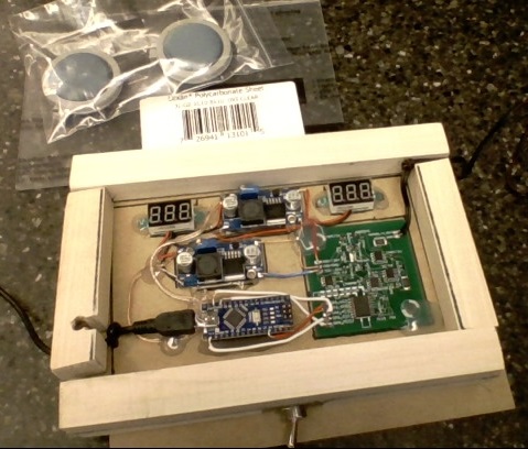
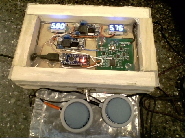
WHENEVER I SAY GLUE I MEAN HOT-MELT GLUE!
[ -- Used in step -- ]
Hot-melt glue
Duct tape
1x (203mm x 132mm x 5mm) medium-density fiberboard (MDF), goes under the device's battery compartment
1x (203mm x 132mm x 2.36mm) polycarbonate sheet (I used "Lexan" type)
2x (203mm x 20mm x 20mm) square dowel
1x (90mm x 20mm x 20mm) square dowel with keyhole to accomodate USB cable as shown
1x (90mm x 20mm x 20mm) square dowel with bevel cut to accomodate output leads
[ -- Procedure -- ]
Tie a knot in the TENS (red/black 2mm pin) output leads; position the knot so it falls just within the corner of the black guideline. In case you're wondering, the knots in the output and input leads are to function as strain relief, and will be glued to the case border. That way, if the cable gets yanked on, the stress is stopped at the knot and case border, and the soldered part isn't put under tension.
Glue the square dowels to the tES device. Glob extra hot glue around the knots, and make sure to fill all gaps between the dowels. We're sealing the upper compartment so that the device will continue to limit the current through the human even if someone spills soda on it while it's turned on. Peel the protective layers off the polycarbonate sheet. With the voltage indicators facing up, run a bead of hot glue all around the top of the square dowels and then (quickly, before it cools) press the polycarbonate sheet down onto it. The top compartment of the device should now be sealed, but the indicator lights, wiring, et cetera will be visible.
Duct tape the rectangle of MDF to the bottom of the device, under the battery compartment. You will need to access the battery compartment to change the batteries! DO NOT GLUE THE MDF TO THE BOTTOM OF THE DEVICE!
Replace batteries when output the voltage indicators read less than 4V. This recommendation holds for both disposable and rechargeable cells. Note that some panel meter voltage indicators sold on ebay are not rated to measure under 4.5V. Use 9 grams of salt (sodium chloride, table salt) per 1 liter of water for the saline solution for the sponge electrodes.
Here Be Dragons
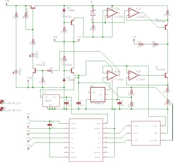

You have completed the necessary reading to build, test, and use the device. As you continue reading, things will become abruptly more abstract, and then gradually more concrete, as the design of the device coalesces before you. Then you'll hit the software and it'll become abstract again.
If you have read and followed the steps up to this point, you will have a working transcranial electrical stimulation device. From here on, I will explain the deeper theory of how the device was designed, and how it operates. This information is useful to customize the device, and for your general understanding.
If the schematic, graph, and hexidecimal code values displayed above this step pique your interest, read on...
Two Current Sources, a Load, and Some Guy Named Kirchhoff

Consider two current sources with a load resistor connected as shown. By Kirchhoff's Current Law, the sum of the currents into a node must equal the sum of the currents out of the node. So I_top = I_bottom + I_load, which we can rearrange algebraically to be I_load = I_top - I_bottom. In the first schematic shown, we are given values for I_top (2.5mA) and I_bottom(2mA), so we find I_load to be 0.5mA.
If we make the bottom current source variable based on a control voltage, Vctl, such that I_bottom = (Vctl / 1.0866) mA, we can smoothly vary I_load between +2.5mA and -2.1mA by varying Vctl between 0V and 5V. This circuit allows you to control the current through the load based on a control voltage, Vctl, with a fixed current source and a voltage-controlled current sink. After we add extra circuitry to cut that output current range down to +/- 2.1mA, the load will be some saline-soaked sponges and a human head! (about 4.7kOhm)
Practical Current Sources and Sinks

Precise current sources and sinks may be built using op-amps and transistors as shown. While BJTs, bipolar junction transistors, are shown in this schematic, appropriately N- or P-channel MOSFETs will work as well*. The load current I_load will be roughly equal to V_ref / R_sense. Error comes from -- among other places -- the base current in the transistor; this error is usually <1% for a typical small-signal transistor. In the design of this transcranial electrical stimulator, darlington pair transistors are used instead of normal BJTs to decrease the error caused by transistor base current significantly, to less than 0.005%.
These current supplies will have a voltage drop of (transistor_V_b_e + V_ref).
*In the circuits shown here, MOSFETs may cause more trouble with spurious oscillations than BJTs.
Failures, Safety Resistors, and Supply Rails
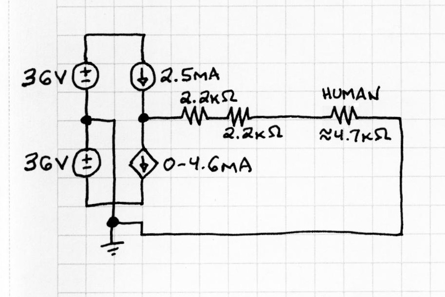
Let's reconsider one of our design specifications. The human head and electrodes have a resistance of 4.7kOhm, so we will design for a worst-case resistance of 9.4kOhm.
We need a bipolar supply for our current sources. This supply must have enough voltage for the current sources/sinks to be able to provide 2.1mA through our human.
The available voltage we need is: V_across_human + V_current_source_drop
Using ohm's law, V=IR,
V_across_human = I_through_human * R_of_human
V_across_human = 2.1mA * 9.4kOhm = 19.74V
Now we need V_current_source_drop.
V_current_source_drop is V_ref_max + V_transistor_base_emitter
5V + 1.4V = 6.4V (our actual V_transistor_base_emitter will be a little lower, but we're designing for the worst-case value)
So the total required voltage is 26.14V.
However, we need to add some safety protection. In the image above, you see two extra resistors, each 2.2kOhm. These are for safety. The reason there are two resistors in series is so that even if one somehow fails short-circuit, there will still be a limiting resistor present. I've never seen a short-circuit failure happen with these resistors, but I have seen one (of the part number I specified, 35202K2JT, out of about two hundred 35202K2JTs tested by me personally) fail open-circuit, but that's ok, it's a graceful failure, since the device output current becomes zero (which is safe).
These 2.2kOhm safety resistors do nothing, usually. Actually, they worsen the performance of the circuit by burning off exta voltage. Since V=IR, V_safety_resistor = I_max * R_safety, V = 2.1mA * 4.4kOhm,
V_safety_resistor_loss = 9.24V
The total required voltage thus becomes 26.14V + 9.24V = 35.34V, so we're going to use +/- 36V supplies.
Now let's examine what happens if one of the current supplies fails short circuit. This is equivalent to connecting the input of the safety resistors directly to plus or minus 36V. Regardless of polarity, the current magnitude that flows will be given by 36V / (R_human + R_safety), 36V / (4.7kOhm + 4.4kOhm) = 3.96mA. This is outside of the recommended +/- 2.1mA current limit for human heads, but it shouldn't be enough to cause any permanent damage or memory loss. (ECT, electroconvulsive therapy, uses about 800mA, and DOES cause memory loss; if short-circuit failure of a primary current limiter occurs, this device's safety resistors limit its output current to 0.5% of the current used for ECT)
In the event of a perfect power supply short directly through one of the series pass transistors, a simultaneous open-circuit failure of the other series pass transistor, and a spherical, ideally conducting human attached to the output, the safety resistors will limit the output current to +/-8.2mA.
This device is also designed so you can get it up and running with fewer parts than shown in the instructions. The quick-and-dirty way to power the device is to make a series chain of eight 9V batteries, attach the ends of the chain to plus and minus 36V (isolated), and then tap the middle of the battery chain (battery battery?) for ISO/GND. Note that more current is drawn from the negative supply than the positive one, so a chain of batteries like this won't drain evenly, the bottom four will drain faster.
Making It Real

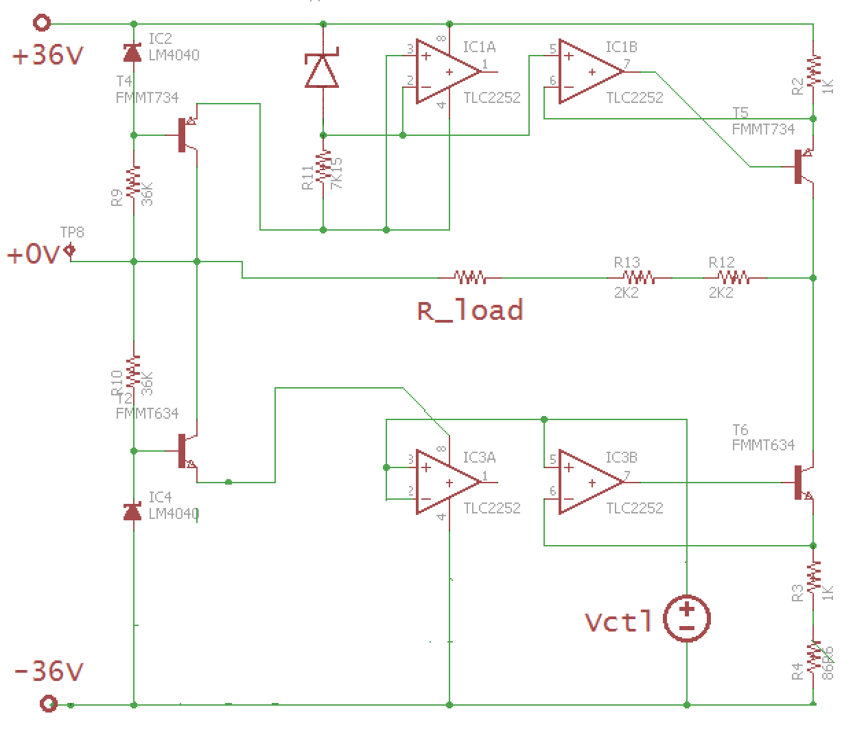
Now we're going to turn the theoretical pieces we've examined so far into a design with real-world parts. This is the design of the device's output stage, which takes a bipolar power supply (+36V / +0V / -36V) and a control voltage (Vctl, between 0V and 5V referenced to the -36V supply rail), and uses them to produce a precise voltage-controlled current between +2.5mA and -2.1mA (we'll cut that range down to +/- 2.1mA later). The op-amps are dual because an additional op-amp is required to cut the output current range, and I attempted to keep the parts count down. Only a single op-amp is used on the +36V rail's current source, but specifying a single op-amp there would increase the number of unique parts in the design, for minimal cost savings, which needlessly makes inventory, ordering, and populating the board more difficult.
The op-amp power supplies are 8.6V, about, op-amp power supply voltage is not critical as long as:
1) op amp max supply voltage,16V for our TLC2252s, is not exceeded
2) there's enough voltage to drive the current sink. For us, 6.4V; 5V maximum dropped across the resistors R3 and R4 + 1.4V worst-case V_b_e of the darlington pair transistor + op-amp headroom (0V for us, TLC2252s are rail-to-rail ^.^ )
Op-amp power supplies are taken from simple emitter follower voltage regulators, AKA transistor series voltage regulators; the voltage regulators get their voltage reference from modern integrated shunt voltage references -- these integrated references are electrically equivalent to zener diodes but perform orders of magnitude better in terms of precision and V/I curve knee sharpness. Vref is also taken from a (precision) integrated shunt voltage reference. As Maxim says, "[a shunt reference] is similar in concept to a zener diode, but has much better specifications."
There are lots of factors to consider in the real world, and I have calculated them, but I'm going to leave it to the reader to pursue the part-by-part level of analysis, should they wish to. Each component has its own power dissipation rating and worst-case power dissipation in this circuit, and it's necessary to check all of them to make sure the design is safe. I checked this design for safe levels of power dissipation twice: first, I drew the entire device schematic on giant 100cm x 50cm quadrille paper, annotated the schematic with worst-case currents through each branch, calculated the power dissipation for each part, and verified that power dissipation was safely within each component's rated limits. After double-checking my theoretical calculations and the component datasheets to ensure calculated design power was within each part's rated limits, I built the prototype and left it fully on for about an hour, and poked each part with a finger. No part was unpleasantly hot. (Semiconductors are actually OK to run unpleasantly hot, die temperature is allowed to go up to 100 C for most devices, but if you can touch everything on your device without discomfort after running it for a long time then the semiconductors will be within a healthy 30 C safety margin. READERS WILL REMEMBER NOT TO USE THIS TECHNIQUE ON HIGH-VOLTAGE DEVICES)
V_CTL comes from a DAC7311IDCKR. We'll talk about our DAC7311 in more detail once we're in the software section. For now, all you need to know is that it has an output that goes between 0V and 5V, requires precisely regulated +5V / +0V power supply rails, and the DAC7311 takes three input lines, named *CS, SCK, and MOSI
(or *SYNC, SCLK, and D_IN, respectively, depending on who you ask...)
Clipping That Current Range

Our DAC7311 is "well behaved". It will always turn on with 0V output. However, for the design we've been considering up until now, that 0V DAC output (DAC output is Vctl) would lead to +2.5mA output current, which is a bit high, and also a really lousy default. Really, we want our device to output 0mA when it powers on with no data signal applied.
Easy. We turn off the entire +36V rail (and thus the fixed 2.5mA positive current source) when the DAC output, AKA V_CTL, is less than 0.435V. That way, the device will power on with 0mA output, gradually lower to -0.4mA output as the DAC output, Vctl, rises, and then at a critical point, 0.435V DAC output, the +2.5mA fixed supply will turn on, bringing the output up to +2.1mA. From 0.435V up to +5V Vctl (DAC output voltage), the output current will linearly decline to -2.1mA. This comparator-derived rail-switching command signal is passed from the (weak, low-voltage) op-amp through (hardy, high-voltage) resistor-transistor logic inverters to switch the +36V rail.
In the device, when the positive rail is turned on, the amber indicator LED lights.
Here's how this solution is inelegant, and why that doesn't matter:
Turning off -- and on -- the *entire* +36V rail is not a gentle thing to do with the circuitry. The positive regulator's op-amp experiences a turn-on transient each time the rail is switched, and there is ringing around this change in state, too. Furthermore, the use of an internally compensated op-amp as a comparator is a poor choice; internally compensated op-amps are slow comparators because of their built-in low-pass filters, and garden variety op-amps are designed to be operated closed-loop, usually (as opposed to comparators, which are open-loop); normal op-amps will be much slower to recover from open-loop saturation (being flung to the ends of their output voltage range) than comparators are.
However. As this device is designed, in normal operation, the positive rail is always on. This rail-switching circuitry is only active when the device is first turned on, before any data is supplied to it. The first thing the control program does is to fill the data buffer with values that cause the current source and sink to be exactly balanced, which sets the device to output 0mA but puts it in the middle of its active range. From that point forward, the +36V rail remains on, so its inelegant transient behavior can be safely ignored.
Isolation Is Safer Than Connection
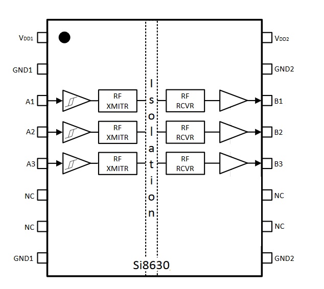

Adding isolation is pretty easy. We use a part called a digital isolator, specifically the SI8630BD-B-IS. This nifty thing passes three digital channels (for us, the 3-wire SPI bus, *CS, SCK, and MOSI) without an electrical connection. The left side gets one supply and ground (2.5V - 5V), and the right side gets another (2.5V - 5V). As a side effect, we can connect this board to any SPI source (up to 50MHz) with any logic voltage between 2.5V and 5V, no level shifter or extra parts required!
The circuitry connected to your head needs to be electrically isolated from the AC line. There are lots of good reasons for this, but let me outline a worst-case scenario that should make the necessity for electrical isolation clear:
Assume you use this device with an AC line connected computer. Let's say the people who wired your computer's outlet somehow accidentally connected the earth pin to the hot conductor of the AC line. If the USB ground of the tES device were directly connected to the HUMAN_GND terminal, and while using the device you touched a metal sink or other earth-grounded object, current would then flow through your body between the HUMAN_GND electrode and the earth ground you were touching. This would be highly unpleasant and/or lethal. Electrically isolating the device's output prevents this risk and several others.
Medical devices are required to follow stringent safety standards. According to IEC60601-1, clause 2.1.5, this device has "Type BF" applied parts (the bits connected to you), type BF being "Electrically connected to Patient but not directly to heart". However... to actually *read* IEC6061-1 the International Electrotechnical Commission wants me to pay $350 for the privelege of even looking at their standards! Technically 350 Swiss Francs, not US dollars, yes, but as of 2017-03-22, 350CHF = $352.43 US, which is close enough. And that price is only for "Part 1" ... medical things, (drugs, hardware, even just looking at the regulations) appear to be specifically designed to drain your finances.
Luckily, the manufacturer of the isolator I'm using (part number SI8630BD-B-IS) has a freely available whitepaper that states that the isolator family I've chosen for this device is acceptable for use with AC-line-powered medical devices, so it should be acceptable for this isolation application too, as the isolator will be exposed to lower voltages. Unless your house wiring is screwed up, in which case the isolator is specified to be capable of handling that too.
The Full Schematic


We add a sprinkling of filtering capacitors and linear regulators, and there we are!
Download the .zip file at the end of this step for a legible version of the board's schematic. You can also get EAGLE (it's free!) to play directly with the .sch and .brd files found in the github repository. Those .sch and .brd files require a custom library for a few of their parts; it's in the same folder in the repository, named precision_tACS.lbr.
Onward, to software!
Downloads
How Is Vctl Set?
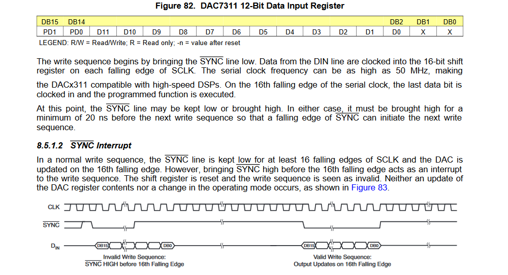

The DAC expects 16 bit SPI writes, SPI mode 1, CPOL=0, CPHA=1, MSB first.
To use the tES device within its recommended operating parameters, restrict the values written to the DAC:
0x06CF < (data written to DAC) < 0x3EC1
As long as the DAC write values are bounded as described above, the device's output will follow the equation:
(OUTPUT_CURRENT)mA = 2.5mA - (0.00028*DAC_WRITE_VALUE)mA
The equation returns results in mA! So to control the DAC easily from within python code:
dacwrite = (int(round(((16383*1.0866)/5)*(2.5-value_in_mA)))).to_bytes(2,byteorder="big",signed=False)
If you have an Arduino/other SPI source of any type up to 50MHz, and any operating voltage between 2.5V and 5.5V (level conversion is automatically performed by the SI8630) on hand you can simply connect its SPI signal (except MISO, the DAC doesn't send any data back) and +VDD/GND pins to the device at the row of 5 pins behind electrical isolation (SPI_VCC, SPI_*CS, SPI_GND, SPI_SCK, SPI_MOSI).
More detail about the DAC itself can be found in the DAC7311 datasheet.
Precise measurements of output current versus DAC write value for this specific device are linked here.
Using an Arduino As a Data Buffer

The Arduino firmware is thoroughly commented and pretty straightforward. The firmware is a simple ring buffer, which holds 256 two-byte values, pushes them out to the DAC every 512 microseconds, and screams "0xFF" over the serial port when it has room for another 128 two-byte values. The only real surprise in the firmware is that the timer interrupt settings for the 512 microsecond delay are really specific, and the device does not perform as would normally be expected if these values are changed, due to hidden interrupt access and modification by the explicitly declared spi.h, and the serial.h built into the Arduino IDE itself.
Changing the timer interrupt settings in the firmware is not recommended unless you have an oscilloscope, and don't mind wading into the 442 page ATmega328 datasheet to cross-reference the TIMSK values (page 211 for TIMSK2, which controls the counter driving the data output timing in the firmware) with the source code of SPI.h and the Arduino software itself.
KludgeGUI

KludgeGUI turned out to be generally user-friendly and relatively bug-free, but if you want features besides those already programmed into it, I recomend that you don't try to extend it, and use this linked python function (also embedded at the bottom of this step) as your starting point, instead.
There's a reason it's called KludgeGUI, after all. Spaghetti code, lots of global variables, minimal commenting, inelegant repetitive code blocks, incomprehensible variable names... "certified operational at 4:55 AM".
However, KludgeGUI does control and display the waveform accurately, even when the output waveform experiences sampling distortion, as seen above.